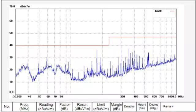
A car dash cam failed radiation emission tests when powered by an external adapter, with excessive emissions detected at 84 MHz, 144 MHz, and 168 MHz. The root cause of the non-compliance needed to be analyzed, and corresponding countermeasures proposed.
01 Preface
A car dash cam failed radiation emission tests when powered by an external adapter, with excessive emissions detected at 84 MHz, 144 MHz, and 168 MHz. The root cause of the non-compliance needed to be analyzed, and corresponding countermeasures proposed.
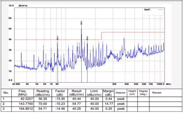
Figure 1 – Radiation test data (spectrum graph and numerical table)]
| No. |
Freq. (MHz) |
Reading (dBuV/m) |
Factor (dB) |
Result (dBuV/m) |
Limit (dBuV/m) |
Margin (dB) |
Detector |
Height (cm) |
Degree (deg.) |
Remark |
| 1 |
82.5257 |
56.39 |
-15.95 |
40.44 |
40.00 |
0.44 |
Peak |
- |
- |
- |
| 2 |
143.7760 |
70.00 |
-15.23 |
54.77 |
40.00 |
14.77 |
Peak |
- |
- |
- |
| 3 |
164.8912 |
54.71 |
-14.46 |
40.25 |
40.00 |
0.25 |
Peak |
- |
- |
- |
02 Analysis of Radiation Source
The product consists of a single PCB with a 12 MHz crystal oscillator. Notably, the excessive emission frequencies are exactly the harmonics of 12 MHz (84 MHz = 12×7, 144 MHz = 12×12, 168 MHz = 12×14).
Further investigation ruled out other potential sources:
- The LCD-CLK frequency was 33 MHz, and the camera MCLK was 24 MHz (neither matching the excessive harmonics).
- Removing the camera did not eliminate the excessive emissions.
- Shielding the 12 MHz crystal oscillator reduced the emission levels significantly.
This confirmed the 144 MHz excessive emission was directly related to the crystal oscillator. The PCB layout is shown below:
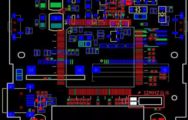
Figure 2 – PCB layout diagram (highlighting the 12 MHz crystal oscillator at the edge)
03 Principle of Radiation Generation
From the PCB layout, the 12 MHz crystal oscillator was placed exactly at the PCB edge. In the radiation emission test environment, capacitive coupling forms between high-speed devices on the tested product and the laboratory reference ground, generating parasitic capacitance and leading to common-mode radiation. The larger the parasitic capacitance, the stronger the common-mode radiation.
Parasitic capacitance essentially arises from the electric field distribution between the crystal oscillator and the reference ground. When the voltage between them is constant, a more extensive electric field distribution results in higher electric field intensity and larger parasitic capacitance.
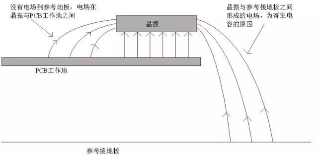
Figure 3 – Schematic of electric field distribution between a crystal oscillator at the PCB edge and the reference ground plane
- Electric field distribution between the crystal oscillator and the reference ground plane (source of parasitic capacitance).
- No effective confinement of the electric field by the PCB’s working ground (GND) plane.
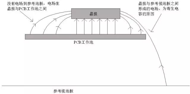
Figure 4 – Schematic of electric field distribution between a crystal oscillator in the PCB center and the reference ground plane
- Most of the electric field is confined between the crystal oscillator and the PCB’s internal working ground plane.
- Electric field leakage to the reference ground plane is significantly reduced, minimizing radiation emission.
When the crystal oscillator is placed in the PCB center (or far from the edge), the internal GND plane effectively contains the electric field within the PCB, drastically reducing leakage to the reference ground and lowering radiation.
04 Countermeasures
- Relocate the crystal oscillator inward: Ensure a minimum distance of 1 cm from the PCB edge.
- Add copper pouring: Pour copper on the PCB surface within 1 cm of the crystal oscillator.
- Connect to GND plane: Link the surface copper pour to the PCB ground plane via multiple vias.
Post-modification test results showed a significant improvement in radiation emissions:
Post-modification radiation test spectrum graph (showing reduced emissions at the previously excessive frequencies)
05 Insights and Takeaways
- Capacitive coupling between high-speed traces/devices and the reference ground plane causes EMI issues.
- Placing sensitive traces or devices at PCB edges leads to susceptibility problems.
- If edge placement is unavoidable (due to design constraints):
- Add a dedicated working ground trace adjacent to the sensitive trace/device.
- Connect this ground trace to the internal ground plane via multiple vias to enhance shielding.
About Maxipcb
Maxipcb empowers innovators to turn cutting-edge technologies into reality.
We offer one-stop solutions for design, simulation, testing, PCB manufacturing, component procurement and SMT assembly, enabling efficient development, rapid deployment and risk control across the full product lifecycle.Serving the world in communications, industrial automation, aerospace, automotive, semiconductor and beyond, we build a safer, more connected future together.


