In PCB design services, communicating requirements with manufacturers and suppliers is the top priority. Requests sometimes lose context because correct information is not provided, sufficient information is not listed, or no information is provided at all. Although experienced PCB designers can take steps to specify all elements they want to see in a PCB stackup, the manufacturer will ultimately make the decision, striving to balance available materials with processing capabilities and yield.
In PCB design services, communicating requirements with manufacturers and suppliers is the top priority. Requests sometimes lose context because correct information is not provided, sufficient information is not listed, or no information is provided at all. Although experienced PCB designers can take steps to specify all elements they want to see in a PCB stackup, the manufacturer will ultimately make the decision, striving to balance available materials with processing capabilities and yield.
A stackup describes more than just the basic structure of a PCB; many other design considerations are built into the stackup, defined by the material properties of your core and dielectric materials. To ensure your design is compatible with the manufacturer’s capabilities, material inventory, and impedance requirements, designers must clearly define their stackup requirements. If you follow my advice when initially creating your design and first ask your manufacturer about their available stackups, you will be in a good position. Designing around that stackup will make collaboration with your manufacturer much easier.
What if you have an existing design and need to produce it anywhere with a compatible material set? How to reduce the risk of receiving non-compliant circuit boards? This is what we will discuss in this article. Following some of these tips will allow you to design with manufacturing, not just for manufacturing.
Ensure PCB Stackup Requirements Are Specified
As mentioned above, in the initial iteration of design, you can usually obtain a standard stackup and use it in your design. This is the fastest way to prototype and move to production. Another option is to design your own stackup using at least your chosen materials, then conduct quality verification with the fabrication house. They will inform you whether it can be produced, and you can decide how to proceed from that step (redesign the stackup or send it elsewhere).
The situation is slightly different when the design is already completed. If you put the design into production, you must ensure the bare board manufacturer can meet multiple specifications, including:
- Layer characteristics: This includes layer thickness, copper weight, copper foil type (reverse-treated, electrodeposited, rolled copper, additive, etc.), and laminate structure/weave style.
- Dielectric and impedance requirements: If there are impedance specifications (signal and power) to be met, you need to specify the dielectric constant in the layer, along with layer thickness and copper.
- Allowed substitutions and tolerances: Manufacturers can see what you permit them to modify to ensure the design can be reliably produced anywhere.
We do not often discuss the third point, instead focusing on DFM as part of the first and second points. If you can account for potential changes required for the PCB stackup in the third point, you can eliminate the risk of receiving out-of-specification circuit boards.
To ensure your PCB stackup requirements are met, you can use a critical document to specify your board requirements: the PCB fabrication drawing. You need to use both a stackup diagram and fabrication notes to convey PCB stackup requirements to the manufacturer.
Start with a PCB Stackup Diagram or Table
In a fabrication drawing, you can immediately specify most stackup requirements using a stackup diagram. This is the simplest method if you want to provide the fabrication house with the basic board requirements. The example below is a 4-layer board design applicable to high-speed PCBs, power regulator modules, microcontroller boards, or other general-purpose boards.
Layer Stack Legend
From this drawing, we can already identify several critical specifications the fabrication house must meet:
- Layer count and layer thickness
- Copper weight for each layer
- Specific material set (ITEQ IT-180BS/IT-180C in this case)
- Gerber file extensions matched to each layer
Sometimes, when I receive a customer’s requirement list, these points are compiled into a stackup document. When submitting design outputs to the manufacturer, stackup files or other requirement files can be part of the document package, but this information should also be reflected in the fabrication drawing. The best approach is to use a stackup diagram as shown above.
What about impedance and dielectric properties? If you designed with a specific material set, you do not need to explicitly list these items, though they can be included in your PCB stackup diagram. To ensure the fabrication house accounts for these tolerances in the design, you must specify acceptable trace width and layer thickness tolerances.
Tolerances for Stackup and Trace Width
To ensure target dielectric constant, thermal/chemical properties, or impedance goals are met (assuming you have specified them), three approaches can be taken in the design:
- Have the fabrication house approve your stackup before any design work. If approved, ensure they specify trace widths for your impedance values based on controlled impedance data. Designing around this trace width and stackup guarantees the specifications you provide in the fabrication drawing will produce the desired electrical behavior.
- Specify IPC stripline compliance for any compatible materials used in the PCB stackup. You need to know the required stripline for the initial material selection.
- Allow the manufacturer to adjust trace widths as needed to accommodate any material substitutions used in the PCB stackup. You do not need to specify a particular stripline or material name, though you may optionally do so in fabrication notes.
Option 1 ensures your board is precise but is limited to manufacturers offering only the specific material set. Options 2 and 3 are more versatile, covering all scenarios, but you may need to request impedance control testing during manufacturing. Implementing Option 2 in fabrication notes is straightforward. The figure below shows an example fabrication note clearly stating which stripline your material set must comply with (Note 16.C, marked in red). Note this method can be used even if impedance control is not required.
In Option 3, your fabrication house may need to adjust these specifications slightly. You need to specify allowable tolerances for layer thickness and trace width in fabrication notes. The example below shows how to specify allowable tolerances for the fabrication house. The red box defines the nominal impedance target initially provided to the fabrication house in the design. The blue box specifies allowable tolerances for trace width and layer thickness.
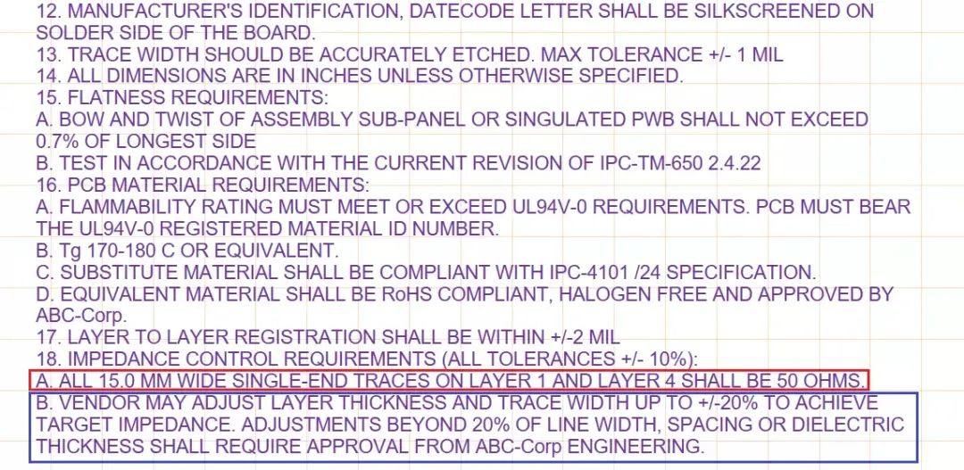
By doing this, you account for the fact that materials used by the fabrication house may have different dielectric constants from those used in your design. Since they cannot always meet the required dielectric constant, they will have to adjust traces to compensate for any major discrepancies that cause impedance to fall outside the specifications defined in Note 18.A.
About Maxipcb
Maxipcb empowers innovators to turn cutting-edge technologies into reality.
We offer one-stop solutions for design, simulation, testing, PCB manufacturing, component procurement and SMT assembly, enabling efficient development, rapid deployment and risk control across the full product lifecycle.Serving the world in communications, industrial automation, aerospace, automotive, semiconductor and beyond, we build a safer, more connected future together.


