Over the past decade, consumer electronics have developed rapidly toward miniaturization, functional diversification, and high-frequency signal transmission. As fundamental components of electronic products, printed circuit boards (PCBs) and high-end packaging substrates are inevitably evolving toward high-density and high-precision configurations.
0 Introduction
Over the past decade, consumer electronics have developed rapidly toward miniaturization, functional diversification, and high-frequency signal transmission. As fundamental components of electronic products, printed circuit boards (PCBs) and high-end packaging substrates are inevitably evolving toward high-density and high-precision configurations. High-density development focuses on realizing multi-layer high-density interconnection, while high-precision development emphasizes fine lines and micro vias. Previously, the improvement priority was placed on line capability; however, as the growth rate of line capability slows down and production costs surge, the development focus will gradually shift to via optimization. Therefore, sufficient attention must be paid to the fabrication and quality improvement of micro blind vias for packaging substrates.
Currently, the mainstream technology for fabricating micro blind vias is laser drilling. With the increasing number and decreasing aperture of blind vias, research on photovia drilling and plasma drilling technologies has also attracted growing attention from research institutions and manufacturing companies.
1 Principles and Applications of Laser Drilling
Laser drilling is classified into infrared (CO₂) laser, ultraviolet (UV) laser, and femtosecond fiber laser according to laser types. The forming principles of different laser drilling methods differ significantly.
1.1 CO₂ Laser Drilling
There are two typical processes for fabricating blind vias on packaging substrates using CO₂ lasers.
The first is
Laser Direct Drilling (LDD). For CO₂ lasers, copper foil exhibits very low absorption at the CO₂ wavelength when irradiated on the copper surface. To enhance the absorption of CO₂ laser energy by copper foil, the copper surface must undergo brown oxidation to increase surface roughness and specific surface area, allowing a large number of electrons in the copper foil to absorb photon energy and generate vibration. If the electron energy is low, phonons in the lattice will constrain the electrons; if the energy is high, secondary radiation occurs, and phonons induce structural vibration. When the material absorbs sufficient energy, intensified vibration gradually stretches intermolecular bonds. Once the mechanical strength of the material is exceeded, the material softens, melts, or even vaporizes, thereby achieving material removal. By optimizing process parameters, Sun Hongchao et al. fabricated through vias with an opening aperture of 70.96 μm and a roundness of 97.26% using direct laser drilling technology, with excellent via reliability.
The second process is Copper Foil Etching and Window Opening (CFM). Before CO₂ laser processing of blind vias, the copper foil on the substrate surface is etched to form windows, exposing the resin material directly to laser irradiation. Electrons inside the resin collide continuously and heat up; when the temperature exceeds the melting point, the resin melts/vaporizes, generating plasma overflow that accelerates evaporation and finally forms a blind via structure.
CO₂ lasers have a wavelength of approximately 10 μm and a pulse width at the microsecond level. Thus, CO₂ laser drilling features high energy input, high drilling efficiency, and good consistency, facilitating control in industrial mass production. Meanwhile, the large heat input inevitably causes thermal ablation or heat-affected zones, generating resin smear on the via wall and bottom, which impairs via reliability. To resolve such issues, post-process desmear is typically adopted to eliminate these defects. However, as the blind via aperture decreases, the chemical exchange efficiency and uniformity of desmear face significant challenges. Additionally, inconsistent ablation time during blind via fabrication inevitably produces inverted-tapered via profiles, which affect subsequent via metallization and signal transmission performance, degrading the performance of high-quality, high-frequency electronic products. CO₂ lasers are generally used for fabricating blind vias with an aperture of 50 μm or larger.
1.2 UV Laser Drilling
The basic principle of UV laser drilling is to utilize the short wavelength and high energy characteristics of UV lasers to break molecular bonds of organic materials, metallic bonds between metals, and ionic bonds in inorganic materials. Through such photochemical reactions, materials are decomposed into particles, molecules, or even atoms. A dust collection system promptly removes loose materials from the irradiated area, completing material removal at the designated region.
UV laser drilling of micro blind vias is a cold processing method that breaks chemical bonds, resulting in high-quality blind vias. UV laser drilling is suitable for small-aperture processing. The minimum spot size of UV lasers for general PCB processing is 15 μm; in practice, the aperture processed by UV lasers is mostly larger than 15 μm. Currently, UV lasers are commonly used for fabricating micro blind vias smaller than 50 μm. By optimizing process parameters, Zhao Cheng et al. reduced the adhesive shrinkage size of adhesive-bearing materials and improved blind via quality. Since both resin and copper foil have high absorption rates for UV lasers, and UV lasers feature short wavelengths and high energy, precise control of laser drilling parameters is required; otherwise, burn-through at the blind via bottom is highly likely to occur. At present, UV laser processing has low efficiency and high production cost for micro blind vias, and is generally used for manufacturing high-value-added products such as packaging substrates. Furthermore, UV lasers show great application prospects in contour cutting and solder mask window opening.
1.3 Femtosecond Laser Drilling
Currently, the pulse width of industrial lasers is mostly at the microsecond or nanosecond level. When processing materials with such long-pulse-width lasers, material removal is generally achieved by absorbing laser energy, generating electron–phonon–lattice heat conduction that heats the laser-radiated area, causing the material to melt or even vaporize. Deng Yunpei et al. found that when the pulse width is in the tens of picoseconds or even nanoseconds, the material damage threshold follows the thermal ablation law with respect to pulse width. When the pulse width is less than or equal to ten picoseconds, the damage threshold deviates from the thermal ablation law, and nonlinear optical effects occur in the material.
A femtosecond laser pulse lasts for 10⁻¹⁵ seconds. Each femtosecond laser pulse focused on the processed material has an extremely high pulse repetition frequency, vaporizing a small amount of material per pulse that is rapidly removed. The vaporized material has no time for heat exchange with surrounding materials, thus avoiding heat-affected zones such as melting, oxidation, and burrs on adjacent materials. This enables precise removal of designated areas, eliminating thermal damage zones such as drilling smear and deformation, and high surface roughness caused by conventional microsecond/nanosecond laser processing, achieving high-precision processing results.
With its ultra-short pulse width and diffraction limit-breaking capability, femtosecond lasers can theoretically fabricate blind vias with the same size as the focused laser spot. Using ultra-short pulse lasers with wavelengths of 355 nm, 532 nm, and 1064 nm, Zhao et al. fabricated through vias with a micro via diameter smaller than 10 μm and a via pitch of 0–2 μm on flexible boards. Ohnishi et al. studied the microfabrication of polyimide films using ultra-short femtosecond lasers. By optimizing pulse duration, repetition frequency, and pulse count, through vias smaller than 10 μm can be fabricated without thermal damage. Using multi-pulse femtosecond lasers, Guo Zhao et al. successfully fabricated micro blind vias on flexible printed circuits (FPCs), proving the feasibility of femtosecond laser drilling on FPC materials, with the prepared micro blind vias reaching a diameter of 2.9 μm. Through orthogonal experiments, Guo Minchao et al. studied the effects of process parameters on micro via quality, and found that high-quality blind vias with an average aperture of 30 μm and a taper angle of 0.24° can be fabricated under the parameters of single-pulse energy 29 μJ, repetition frequency 92 kHz, pulse count 2112, and defocus amount 0.01 mm, enabling fast and high-quality PCB fabrication.
When the laser processing pulse time is shorter than the heat conduction time, heat conduction can eliminate damage and internal stress issues. Femtosecond pulse processing achieves products with minimal thermal damage, no thermal damage, and no thermally induced internal stress. Limited by the diffraction law, the focused spot size cannot be smaller than half the wavelength. However, femtosecond pulse lasers have extremely high peak energy, which induces multi-photon absorption when interacting with materials, breaking through the diffraction limit. The processing scale can be far smaller than the focal spot, reaching sub-micron and nano levels. Femtosecond laser drilling struggles to balance processing precision, quality, and efficiency, which restricts its further development and application.
2 Plasma Drilling Technology
Plasma refers to a partially ionized gas formed by ionizing low-energy gases through an electric field, consisting of positive and negative ions, charged molecules, and atoms, and is electrically neutral as a whole. Plasma features high energy and strong reactivity, capable of interacting with most organic materials, and has thus been applied to PCB manufacturing. Initially, it was used for desmearing after drilling multi-layer circuit boards, especially for desmearing flexible printed circuits. Chemical desmearing is risky for flexible boards because polyimide in flexible circuits has low chemical resistance and is prone to oxidative failure. Plasma treatment not only safely removes smear but also produces a favorable via wall surface morphology. Particularly for cleaning micro blind vias, plasma can compensate for insufficient resin smear removal caused by poor chemical exchange. By optimizing process parameters of radio-frequency plasma, Chen Lei et al. realized the cleaning of through vias with high aspect ratios.
The evolved plasma drilling technology enables controllable etching rates and etching profiles. The etching rate and profile depend not only on the energy and angle distribution of plasma impinging on the etched material, but also on the physical and chemical processes between plasma and the etched material surface.
The fabrication process of plasma drilling is as follows: first, perform window opening on the inner-layer board at the positions where blind vias are to be fabricated using a mask to expose the dielectric layer. Next, place the substrate for blind via fabrication into a plasma vacuum chamber, and etch the dielectric layer into blind vias using highly active plasma gases (such as N₂, H₂, O₂, CF₄, etc.). The type of plasma gas and the mixing ratio between gases significantly affect the etching rate of different dielectric layers.
Plasma drilling features strong processing capability; theoretically, it can fabricate blind vias with the same size as the window opening, and offers high flexibility in blind via fabrication, allowing simultaneous processing of multiple via sizes. Plasma itself has excellent cleaning performance; as long as etching reaches the blind via bottom, the desmear process can be omitted. In addition, the plasma-treated surface has high activity, which helps improve the efficiency and reliability of blind via fabrication.
Conventional reactive plasma etching is isotropic when reacting with organic materials, so undercutting easily occurs during dielectric layer etching, turning blind vias into drum-shaped profiles, which poses great difficulties for subsequent via metallization. With the maturation of plasma drilling technology, plasma drilling capable of anisotropic etching has emerged.
The author conducted research on plasma drilling: window openings of different sizes were fabricated on substrates, and the feasibility of plasma drilling was evaluated by comparing dielectric layer etching results on different plasma equipment, as shown in
Figure 1. Blind vias fabricated by conventional plasma etching exhibit an obvious "bulging belly" cross-section, indicating isotropic etching of plasma gas, which etches downward while causing significant horizontal copper overhang, failing to meet industrial requirements for blind vias. Blind vias fabricated by improved plasma etching equipment feature steep and straight via walls, nearly vertical downward etching with minimal undercutting, facilitating the fabrication of qualified blind vias. After electroless copper plating and electroplating, blind vias with compliant profiles and tight bonding between electroless copper, via bottom, and base copper are obtained.
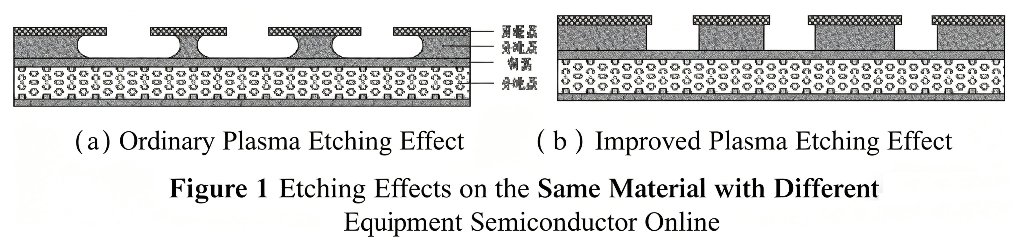
(a) Conventional plasma etching effect
(b) Improved plasma etching effect]
Plasma drilling can be used to fabricate blind vias within the window opening capability, with favorable profiles and high roundness, making it a feasible micro blind via fabrication technology. However, plasma drilling has low efficiency; the current etching rate is several hundred nanometers per minute, limiting its application to thin substrates. More suitable gas media need to be developed to increase the etching rate. Meanwhile, plasma etching equipment is mainly wafer-level, and the lack of large-size (panel-level) equipment hinders the further development of plasma drilling.
3 Photovia Drilling Technology
Photovia drilling uses a UV exposure machine to selectively expose a photosensitive resist film. The exposed areas undergo polymer decomposition, while the unexposed areas remain unchanged. The decomposed polymer is removed by developer, achieving material removal at selected areas. Subsequently, blind vias of corresponding sizes are fabricated through electroless copper plating and electroplating filling. Using photosensitive ink, Kawamoto Mineo et al. realized the fabrication of through vias with a diameter of 60 μm and build-up layers.
Photovia drilling fabricates blind vias through the process of lamination → exposure → development → electroless copper plating → electroplating, as shown in Figure 2.
This method can fabricate micro blind vias of various sizes in one exposure, with low heat input and high blind via quality. Photovia drilling has not been widely used in mass production, partly due to its reliance on photosensitive dielectrics with limited optional types. Meanwhile, early photovia materials were mostly liquid photosensitive inks, which easily caused via position deviation. At present, Japanese companies have developed dry-film photosensitive resist dielectrics, enabling more convenient photovia drilling. Direct imaging (DI) exposure machines realize precise alignment and micro blind via fabrication, solving part of the industrialization issues.
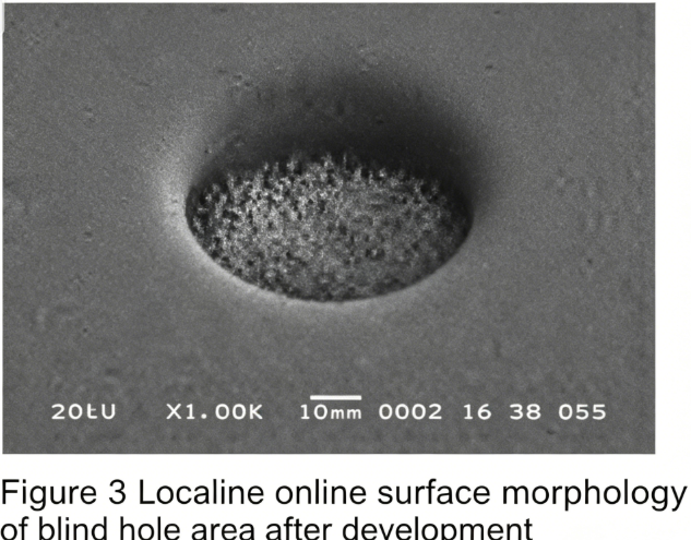
The author conducted feasibility research on photovia drilling by exploring different process flows. The blind via area obtained after exposure, lamination, and development of dry-film photovia materials is shown in Figure 3. The photovia material surface is extremely flat with low roughness, and the blind vias feature high roundness and straight walls, providing an excellent foundation for blind via fabrication.
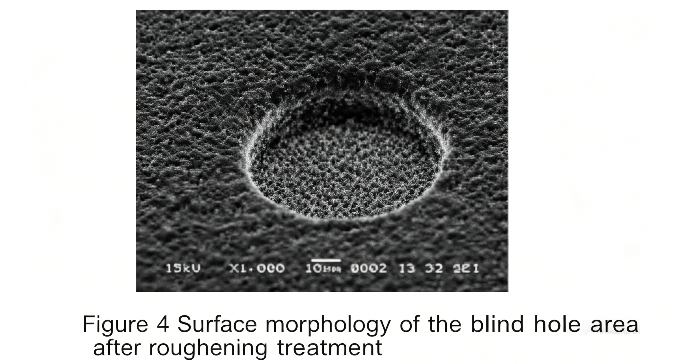
Photovia drilling adopts the semi-additive process, requiring subsequent electroless copper plating and electroplating on the photovia material. Therefore, ensuring the adhesion between the photovia material and electroless copper, as well as between the blind via bottom copper and electroless copper, is critical. Generally, the surface of the photovia material needs to be roughened, and a small amount of residual photovia material at the blind via bottom is removed. The surface morphology of the treated blind via area is shown in Figure 4. The roughness of the photovia material surface and blind via sidewalls increases significantly, enlarging the specific surface area and facilitating electroless copper deposition. The copper surface profile at the blind via bottom is also clearer, indicating thorough removal of contaminants on the copper surface. Subsequent electroless copper plating, lamination, and electroplating processes can fabricate blind vias of approximately 50 μm. This proves that photovia drilling is indeed feasible for fabricating micro blind vias. It not only greatly shortens the blind via fabrication time but also produces small-sized, high-quantity blind vias with arbitrary size combinations, making it one of the future development directions of micro blind via fabrication.
Insufficient adhesion between electroless copper and photovia materials remains a key factor limiting the industrial application of photovia drilling, as poor adhesion reduces the thermal reliability of packaging substrates. To improve the adhesion between the metal layer and substrate, researchers have begun to use sputtered Ti-Cu seed layers instead of electroless copper plating. This method significantly enhances the adhesion between the seed layer and substrate, but has not been applied in large-scale mass production of packaging substrates due to cost and equipment constraints.
4 Conclusion
This paper summarizes the commonly used micro blind via forming technologies for packaging substrates, focusing on the principles of different types of laser drilling, plasma drilling, and photovia drilling, and analyzes the respective advantages and limiting factors of each forming method. With the increasing number, decreasing size, and higher quality requirements of micro blind vias in the packaging substrate field, more sophisticated micro blind via processing technologies must be developed.
About Maxipcb
Maxipcb empowers innovators to turn cutting-edge technologies into reality.
We offer one-stop solutions for design, simulation, testing, PCB manufacturing, component procurement and SMT assembly, enabling efficient development, rapid deployment and risk control across the full product lifecycle.Serving the world in communications, industrial automation, aerospace, automotive, semiconductor and beyond, we build a safer, more connected future together.

 (a) Conventional plasma etching effect
(b) Improved plasma etching effect]
(a) Conventional plasma etching effect
(b) Improved plasma etching effect]

