Just as code needs readability, so do schematics. Schematics are often shared with other engineers, and poor readability leads to communication issues. Developing good habits to create standardized schematics is crucial. An excellent schematic also considers testability, maintainability, BOM normalization, and more.
Just as code needs readability, so do schematics. Schematics are often shared with other engineers, and poor readability leads to communication issues. Developing good habits to create standardized schematics is crucial. An excellent schematic also considers testability, maintainability, BOM normalization, and more.
1. Divide into Functional Modules
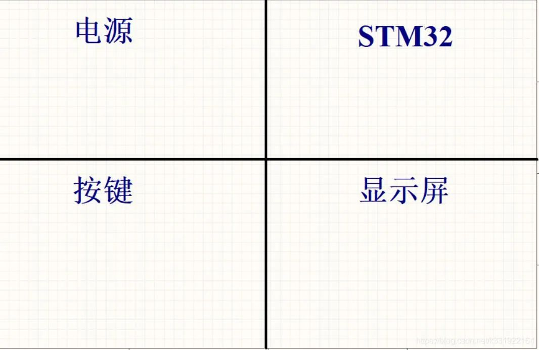
Schematic divided into labeled functional modules with dividing lines
Divide the schematic into distinct areas with lines and label each with its function (e.g., Power Supply, STM32). This helps others understand the circuit quickly and simplifies debugging/repair by locating problem-related modules easily.
2. Label Key Parameters
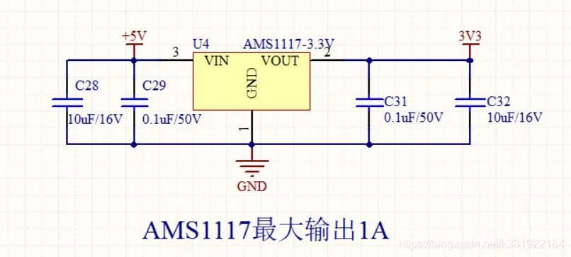
AMS1117-3.3V regulator circuit with labeled maximum output current
Label critical parameters (e.g., maximum output current, input voltage range, operating temperature, truth tables for digital circuits). This helps others modify the circuit by understanding load capacity and performance limits.
3. Annotate Resistors/Capacitors/Inductors/Ferrite Beads
(1) Resistors
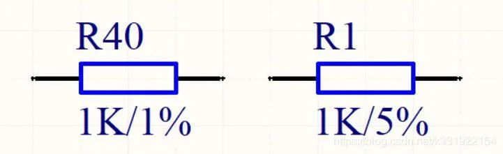
Resistors labeled with resistance and tolerance
Mark resistance and tolerance for every resistor; add power rating for high-power resistors. Use
1% precision for switching power supply sampling resistors and op-amp circuits;
5% precision is sufficient for pull-up/down resistors.
Note: Write resistance as
1K instead of
102 to avoid unit conversion for readers.
(2) Capacitors
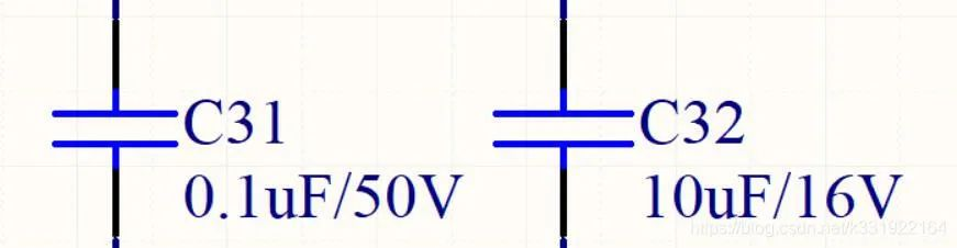
Capacitors labeled with capacitance and voltage rating
- C31: 0.1uF/50V
- C32: 10uF/16V
Mark capacitance and voltage rating; add precision or material (e.g., X7R, Y5V, NP0 for ceramic capacitors) for high-precision capacitors.
Note: Write capacitance as
1uF instead of
105.
(3) Inductors
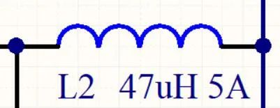
Inductor labeled with inductance and saturation current
Mark inductance and saturation current for all inductors.
(4) Ferrite Beads
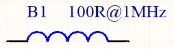
Ferrite bead labeled with impedance and corresponding frequency
Mark impedance and the frequency it is rated for (ferrite beads have frequency-dependent impedance).
(5) Other Components
Extend the same rule to all components (e.g., Crystal: 8MHz/50ppm).
4. Improve Maintainability
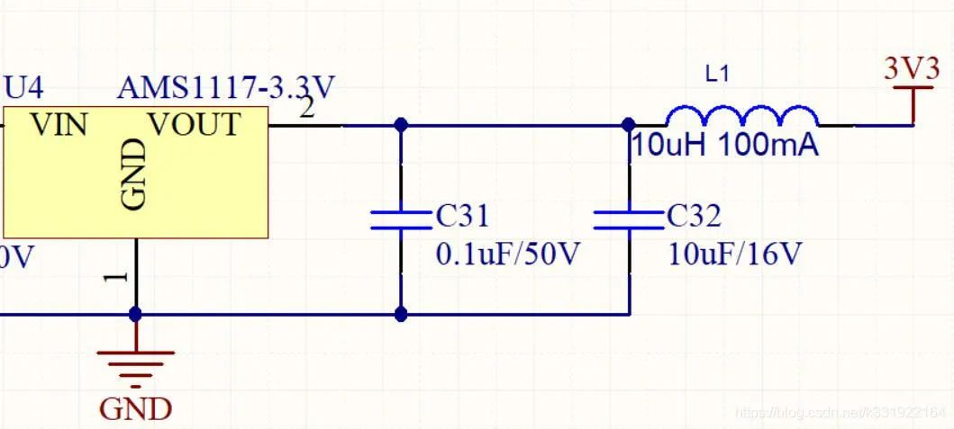
AMS1117 circuit with a series inductor for maintenance
Add series components (inductor, ferrite bead, or 0Ω resistor) to disconnect circuits for fault diagnosis during repair. Exceptions: Omit if the load is too large (high-power components increase cost) or the circuit is low-risk. Add for high-pin-count packages (e.g., QFP64) with higher soldering failure rates.
5. Normalize the BOM (Bill of Materials)
Minimize component types to reduce the purchaser’s workload and production issues.
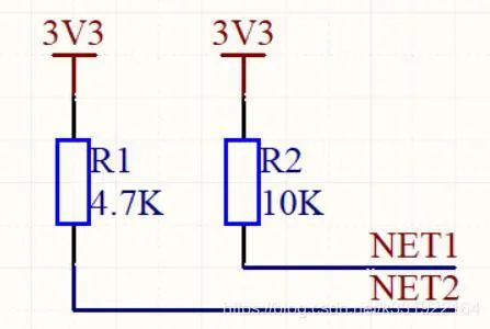
Two pull-up resistors (4.7K and 10K) merged into 10K for BOM normalization
Unify non-critical components (e.g., merge 4.7K and 10K pull-up resistors into 10K; standardize decoupling capacitor values). Apply this rule to all passive components.
6. Power and Ground Symbols
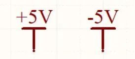
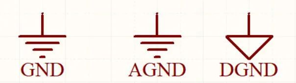
Power symbols with voltage values and ground symbols (GND/AGND/DGND)
- Power: Label voltage values (e.g., +3V3, +5V) for single/double power systems; avoid vague labels like
VCC.
- Ground: Use
GND for a single ground plane; AGND (analog) and DGND (digital) for separated grounds. Use unique symbols for video/audio ground in dedicated systems.
Note: Do not hide net names (e.g., AGND) to avoid connection errors.
7. Add Test Points
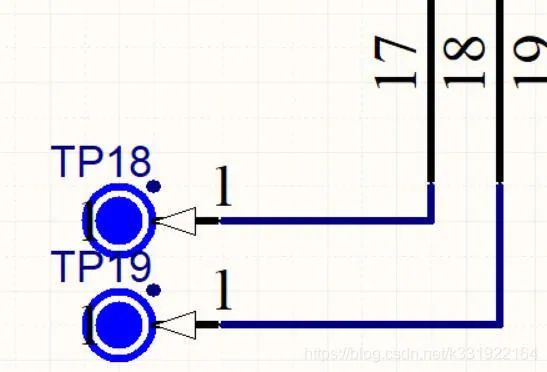
Schematic with labeled test points (TP18, TP19) as exposed copper pads
Add test points (TP, exposed circular copper pads) for hard-to-measure pins (e.g., QFP, BGA, QFN packages) to facilitate oscilloscope probing and debugging.
8. Standardize Net Labels
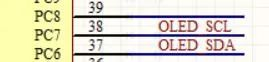
I2C net labels for OLED with component prefix: OLED_SCL, OLED_SDA
- Add component prefixes to net labels (e.g.,
DS18B20_DATA for temperature sensor, OLED_SCL for OLED I2C) to avoid conflicts and improve readability.
- Use UPPERCASE for all net labels.
9. Design for Fault Tolerance/Compatibility
Fault Tolerance
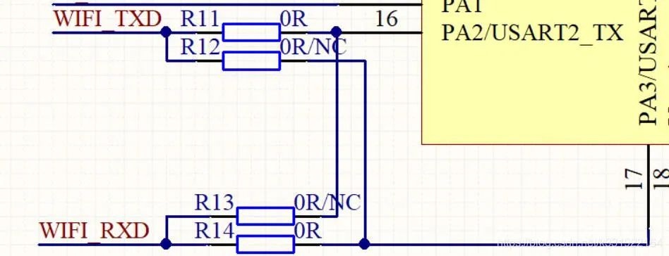
UART circuit with four resistors for reversible RX/TX connections
- Solder R11/R14: RX-RX, TX-TX (cross-connection)
- Solder R12/R13: RX-TX, TX-RX (direct connection)
- Remove resistors and hardwire after debugging.
Add reserved circuits to resolve uncertain connections quickly without delaying the project schedule.
Compatibility
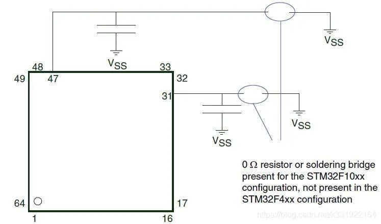
STM32F103/F407 compatible circuit with 0Ω resistor jumper
- Solder 0Ω resistor: STM32F103 configuration
- Solder capacitor (omit 0Ω): STM32F407 configuration
Design compatible footprints for alternative chips (e.g., STM32F103/F407) to avoid re-spinning the board for component swaps.
10. Define NC and NF Clearly

Schematic with 0Ω resistor labeled OR/NC
- NC (Not Connect): Pin/component is unconnected.
- NF (Not Fix): Component is not mounted (reserved footprint).
Note: NC may also mean Normal Close for relays/contactors—interpret based on context.
11. Mark Version Changes
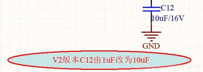
Capacitor C12 labeled with version change: V2: 1uF → 10uF
Explicitly mark component/parameter changes for each version (e.g., V2: C12 changed from 1uF to 10uF). This enables traceability for fault analysis and revision control.
12. Label Floating Pins
Floating chip pin marked with an "X"
Mark all unused/floating pins with an X to avoid accidental connection and clarify intentional floating.
13. Add Scalability
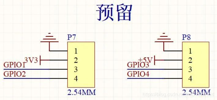
Schematic with reserved GPIO pins on 2.54mm headers labeled "Reserved"
Reserve GPIO pins, headers, or circuits for future functional upgrades. This avoids re-spinning the board when requirements change and allows quick validation of new features.
14. Design for Error Prevention
Unkeyed Connectors
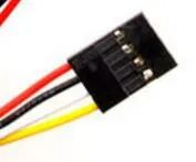
4P Dupont connector with two possible wiring sequences (red-black-white-yellow / yellow-white-black-red)
Unkeyed connectors (e.g., Dupont) risk reverse power/ signal connections, which may damage components. Solve this with three methods:
- Use keyed connectors: USB ports, aviation connectors (best practice).
- Symmetric design: [Illustration: Symmetric pin layout for error-proof connection] Arrange pins so reverse connection does not cause damage (higher cost).
- Rectifier bridge for DC power: [Illustration: DC power input with MB8S rectifier bridge for polarity protection] Add a rectifier bridge to ensure correct voltage polarity regardless of input wiring (common in access control systems; consider cost/power loss).
15. Indicate Signal Flow
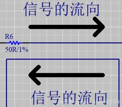
Directional coupler circuit with labeled signal flow arrows
Mark signal flow with arrows for analog/RF circuits (e.g., directional couplers, amplifiers) to clarify signal transmission paths and avoid miswiring.
16. Add PCB Routing Recommendations

Differential pair net labels with routing rules: NETN/NETP, equal length, 6mil width, 6mil spacing
If another engineer will design the PCB, add routing guidelines directly on the schematic (e.g., differential pair rules: equal length, line width/spacing; impedance-controlled traces; ground plane requirements).
17. Use # for Inversion (Instead of ¯)
[Illustration: Net label comparison: CLK¯ (easily blocked) vs CLK# (clear)]
Avoid using an overbar (
¯) for inverted signals—it can be blocked by wires in schematic software, leading to connection errors. Use
# instead (e.g.,
CLK# for inverted clock).
About Maxipcb
Maxipcb empowers innovators to turn cutting-edge technologies into reality.
We offer one-stop solutions for design, simulation, testing, PCB manufacturing, component procurement and SMT assembly, enabling efficient development, rapid deployment and risk control across the full product lifecycle.Serving the world in communications, industrial automation, aerospace, automotive, semiconductor and beyond, we build a safer, more connected future together.


