Integrated circuits can be packaged in a variety of ways when cut from a silicon wafer, including Dual In-line Package (DIP), Small Outline Integrated Circuit (SOIC), Thin Quad Flat Package (TQFP), Quad Flat No-leads (QFN), and Ball Grid Array (BGA).
Integrated circuits can be packaged in a variety of ways when cut from a silicon wafer, including Dual In-line Package (DIP), Small Outline Integrated Circuit (SOIC), Thin Quad Flat Package (TQFP), Quad Flat No-leads (QFN), and Ball Grid Array (BGA).
In different plastic packages, the connection between the silicon IC and the package pins is achieved through a technology called wire bonding.
DIP packages are larger and easier to solder manually (more suitable for hobbyists), while BGA packages cannot be soldered manually and require special equipment for assembly onto a PCB.
BGA packages feature the highest pin density, meaning they occupy the smallest space on a PCB—an essential characteristic for most modern high-end electronic products such as smartphones. However, such high-density packaging requires special techniques to route all signals onto the PCB.
The following are some general techniques for routing BGA chips during the PCB design process.
Design Rules
Even before starting PCB layout, the first step is to define the design rules:
- How many layers will the board have?
- What is the minimum trace width?
- What is the minimum trace spacing?
- What is the minimum via size (minimum drill diameter and minimum annular ring)?
Generally, more layers and tighter feature tolerances make PCB routing easier. However, more layers and stricter tolerances usually also make the board more expensive (and slower to manufacture).
Production Volume
One determining factor is the expected production volume—how many such boards are projected to be produced? For high-volume products, it may be worthwhile to invest extra effort in careful routing with the fewest possible layers to reduce the cost per PCB. For low-volume products, the labor cost of spending additional time routing for fewer layers is not justifiable.
It is also necessary to check the capabilities of your PCB manufacturer and whether they can actually produce boards that meet your design specifications, i.e., their minimum trace width, trace spacing, drill size and annular ring specifications (as well as the maximum number of board layers they can produce).
Impedance Requirements
Another factor is impedance requirements and whether any (many) traces need a specific impedance, as trace width, trace spacing and layer stack will determine trace impedance. Additionally, it goes without saying that some inner layers of the board will be power reference planes (for constant impedance); check our high-speed design articles if you are unfamiliar with this.
Some BGAs (such as Microprocessor Units (MPUs)) have multiple power domains, and the power planes on the inner layers of the board are usually divided into different sections according to the power connections used in specific areas of the chip. For example, DDR memory may operate at a specific voltage and will have a power placement spanning the DDR chip and the DDR section of the MPU, while the SD/eMMC section will operate at a different voltage and have its own power placement spanning that memory and the corresponding section of the MPU.
A proper power plane beneath the relevant pins is important for impedance matching, but also simplifies routing for these pins, as they only require a via down to the power plane (instead of a trace routed outside the BGA area).
Component Documentation
Sometimes, IC datasheets provide recommendations on design rules, such as an excerpt from STMicroelectronics' STM32 MP1 application note on getting started with the hardware design of this processor:
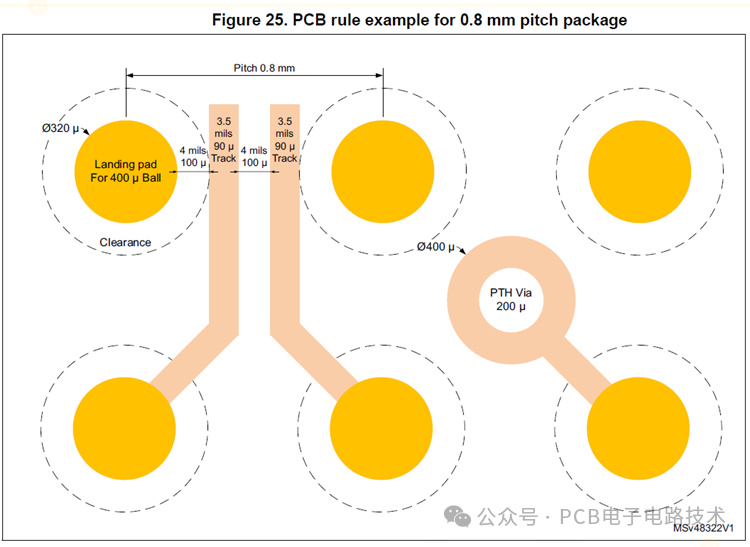 Figure 25. PCB rule example for 0.8 mm pitch package
Pitch 0.8mm / 0320 mils
Landing pad: 4mils
Clearance: 3.5 mils
PTH Via: 200
Track 90: 4mils 100, 4mils 100
400 Ball / MSv48322V1
In general, it is mandatory to check the component documentation for any design requirements or recommendations. There may also be specific design constraints for routing certain parts of the design, such as impedance and spacing requirements on DDR connections.
When extracting the PCB package footprint from the library, it is necessary to check the BGA pad size of the imported device—generally, these sizes should be 80% of the BGA ball diameter, but this is not always set when importing the package footprint.
BGA chips almost always require decoupling capacitors and may also need calibration resistors placed close to the chip (usually directly underneath it), so determining the package size of these capacitors is also an important step that should be completed in advance. Similarly, smaller package sizes make routing easier, but the equipment and processes required for PCB assembly become more advanced (and thus potentially more expensive).
Another source to check when defining design rules is the chip's reference design board. Regardless of the PCB design software used, manufacturers typically provide the board's Gerber files, which can be opened and inspected with Gerber viewing software such as ViewMate. The number of layers, trace width, trace spacing and via size can all be verified.
Via Options
Another potential design decision is whether to use blind and/or buried vias, which are also more expensive but make higher-density designs easier (or even possible). Pad via technology is another technique that can be used to increase density, but it also comes with a higher cost.
Placement and Routing
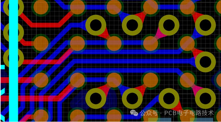
Some BGAs have selectively filled balls, where some ball positions on the BGA are unused to create escape channels for routing traces.
Removing non-functional pads on inner-layer vias helps free up more routing space (when using boards with more than 6 layers).
Vias are usually arranged in a dog-bone pattern.
A technique to increase the density of traces escaping from inner rows is to arrange vias in such a way as to create a channel where multiple traces can be routed in close proximity:
As a final tip, it sometimes helps to not place adjacent chips (such as an MPU and DDR) too close together to leave enough space for length-matched serpentine traces, which usually take up more space than you might expect.
About Maxipcb
Maxipcb empowers innovators to turn cutting-edge technologies into reality.
We offer one-stop solutions for design, simulation, testing, PCB manufacturing, component procurement and SMT assembly, enabling efficient development, rapid deployment and risk control across the full product lifecycle.Serving the world in communications, industrial automation, aerospace, automotive, semiconductor and beyond, we build a safer, more connected future together.

 Figure 25. PCB rule example for 0.8 mm pitch package
Pitch 0.8mm / 0320 mils
Landing pad: 4mils
Clearance: 3.5 mils
PTH Via: 200
Track 90: 4mils 100, 4mils 100
400 Ball / MSv48322V1
Figure 25. PCB rule example for 0.8 mm pitch package
Pitch 0.8mm / 0320 mils
Landing pad: 4mils
Clearance: 3.5 mils
PTH Via: 200
Track 90: 4mils 100, 4mils 100
400 Ball / MSv48322V1
