In the circuit principle design phase, to reduce mutual interference between circuits, engineers generally introduce different GND ground wires as the 0V reference points for circuits with different functions, forming different current loops.
In the circuit principle design phase, to reduce mutual interference between circuits, engineers generally introduce different GND ground wires as the 0V reference points for circuits with different functions, forming different current loops.
01 Classification of GND Ground Wires
Analog Ground (AGND)
It is mainly used in the analog circuit part, such as the ADC acquisition circuit of analog sensors and the operational amplification proportional circuit.
Digital Ground (DGND)
Relative to the analog ground (AGND), it is mainly used in the digital circuit part, such as the key detection circuit, USB communication circuit, and single-chip microcomputer circuit.
Power Ground (PGND)
Analog ground (AGND) and digital ground (DGND) are both for low-power circuits. In high-power circuits, such as motor drive circuits and solenoid valve drive circuits, there is an independent reference ground wire called power ground (PGND).
Power Supply Ground (GND)
Analog ground (AGND), digital ground (DGND) and power ground (PGND) are all classified as DC ground (GND). These different types of ground wires must eventually converge to serve as the 0V reference ground for the entire circuit, namely the power supply ground (GND).
AC Ground (CGND)
It generally exists in circuit projects with AC power supplies, such as AC-DC AC-to-DC power supply circuits.
Earth Ground (EGND)
02 The Principle of GND in Detail
Why is a single GND ground wire divided into so many types, and why is a simple circuit problem made so complicated? Why is it necessary to introduce so many subdivided GND ground wire functions? Engineers usually uniformly name such GND ground wire design issues as GND without differentiation during schematic design, which makes it difficult to effectively identify GND ground wires for different circuit functions during PCB routing, and all GND ground wires are simply connected together directly. Although this operation is convenient, it will lead to a series of problems:
- Signal Crosstalk: If GND ground wires for different functions are directly connected, high-power circuits will affect the 0V reference point GND of low-power circuits through GND ground wires, resulting in crosstalk between signals of different circuits.
- Signal Accuracy: The core assessment index of analog circuits is signal accuracy. Without accuracy, analog circuits lose their original functional significance. The voltage of AC power ground (CGND) fluctuates up and down periodically due to its sine wave, unlike DC ground (GND) which remains at a constant 0V. Connecting GND ground wires of different circuits together will cause the periodically changing AC ground (CGND) to drive the change of analog circuit ground (AGND), thus affecting the voltage accuracy value of analog signals.
- EMC Test: The weaker the signal, the weaker the external electromagnetic radiation (EMC); the stronger the signal, the stronger the external electromagnetic radiation (EMC). If GND ground wires for different functions are connected together, the GND ground wire of the strong-signal circuit will directly interfere with the GND ground wire of the weak-signal circuit. As a result, the originally weak electromagnetic radiation (EMC) will also become a strong external electromagnetic radiation signal source, increasing the difficulty of handling EMC tests for the circuit.
- Circuit Reliability: The fewer the signal connections between circuit systems, the stronger their independent operation capability; the more the signal connections, the weaker their independent operation capability. Imagine two circuit systems A and B with no intersection at all—the performance of circuit system A will not affect the normal operation of circuit system B, and vice versa. If the ground wires of circuits with different functions are connected together in a circuit system, it is equivalent to adding a link for interference between circuits, which reduces the reliability of circuit operation.
03 Step-by-Step Guide to Drawing "GND"
The importance of "GND" on a PCB board is no less than that of water to the human body. How to draw a good "GND"? Just pay attention to the following points.
- Make Zoned "GND"
Different functional modules on a PCB board are distributed in different positions, and the "GND" requirements for the corresponding modules are also different.
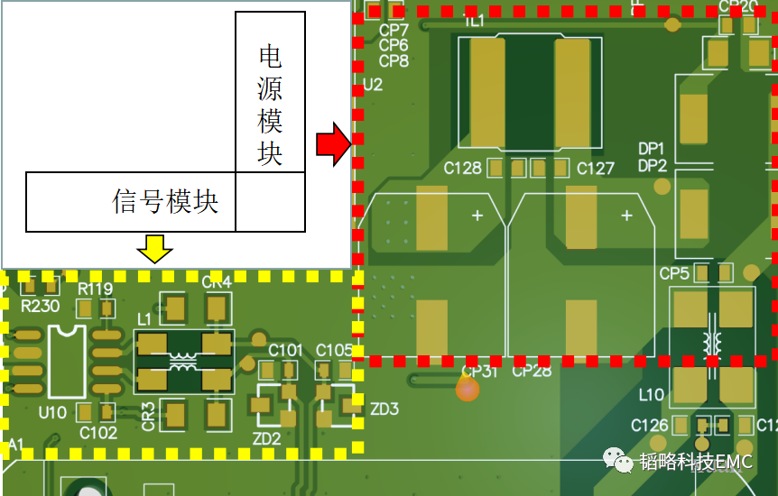
1: PCB layout with conflict between power ground and signal ground
This is a PCB layout with a conflict between power ground and signal ground. In this circuit, the power GND actually acts as the "power negative electrode" rather than the "0V reference ground", while the signal part GND actually acts as the "0V reference ground". In this case, the "unclean" power ground causes interference to the signal part! There are two ways to handle this situation:
① Separate the ground of the signal part from the GND of the power part and do not connect them directly;
② Hollow out the GND of the signal part, and if power supply is needed, supply power by means of wiring.
- Avoid "Stepped" GND
There are also cases of stepped GND where the originally complete GND of a module is divided into multiple areas by other wiring due to structural constraints.
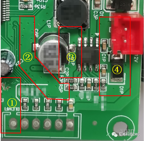
PCB circuit with stepped GND caused by structural constraints
As shown in the following PCB circuit, the negative electrode of the power input is connected to the PCB board and directly becomes "GND" (position ①). On the way to the power module, the area between ① and ② is separated by a signal line; the area between ② and ③ is separated by a 5V output; and the area between ③ and ④ is separated by the chip enable pin. Although the GND with this layout is connected when measured with a multimeter, it is unreasonable in terms of the wiring sequence on the schematic and the "ground impedance" in the high-frequency state. Especially since the power module is one of the core sources of EMC problems, the ground layout must be complete on the same layer!
- Reject "Waist-shaped" GND
When covering copper or laying ground for the entire PCB board, there are often areas where a "waist shape" appears between GND and GND due to wiring or vias in other positions!
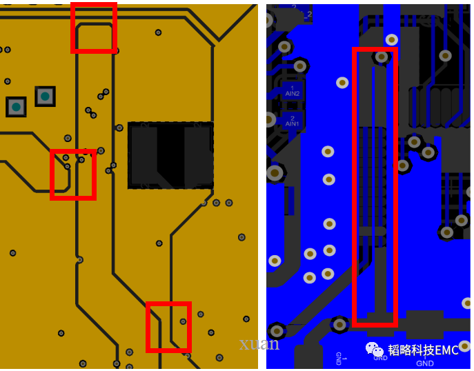
Comparison of "waist-shaped" GND and "pig-tail-shaped" GND
For example, in the following two pictures, the left one is a "waist-shaped" GND and the right one is a "pig-tail-shaped" GND. Both types of GND are not good layouts for EMI and EMS! The "waist-shaped" GND can be widened, or copper laying can be directly prohibited in overly narrow areas. For the "pig-tail-shaped" GND, it is best to cut off the copper laying; if it is required for other functions, add more vias to ensure good grounding.
The "GND" on a PCB board requires engineers to conduct repeated inspections and overall layout considerations. Do not be perfunctory for the sake of convenience, nor ground just for the sake of grounding! When laying copper for "GND", it is necessary to pay attention to distinguishing whether each part of the GND can be laid continuously, whether there is "unreasonable" GND among the dense wiring, and the actual function of "GND" in each area!
About Maxipcb
Maxipcb empowers innovators to turn cutting-edge technologies into reality.
We offer one-stop solutions for design, simulation, testing, PCB manufacturing, component procurement and SMT assembly, enabling efficient development, rapid deployment and risk control across the full product lifecycle.Serving the world in communications, industrial automation, aerospace, automotive, semiconductor and beyond, we build a safer, more connected future together.


