As shown in the figure below, the minimum gap d required between the test point and the pin through hole. The pin of the through-hole device is 125mil.
As shown in the figure below, the minimum gap d required between the test point and the pin through hole. The pin of the through-hole device is 125mil.
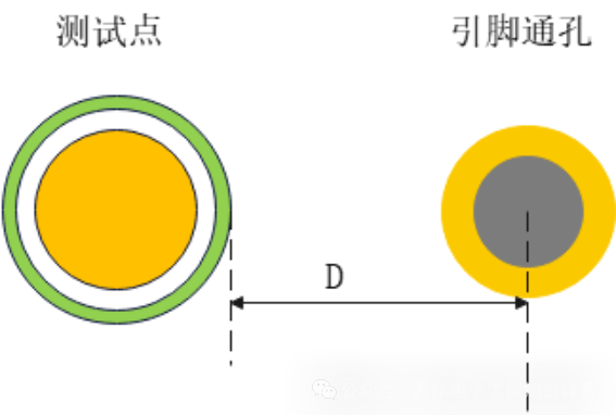
Figure: Pin Clearance from Test Point to Via Device
In PCB design, the gap between the test point and the pin through hole is an important parameter. According to the information you provided, the following are the related contents of the gap between the test point and the pin through hole:
The minimum spacing d is 125mil: this is the minimum acceptable gap between the test point and the pin through hole. This gap is to ensure that there is enough space between the test point and the pin through hole to prevent them from touching each other or short-circuiting.
The gap between the test point and the pin through hole is to ensure that the test point can be normally connected to the pin through hole and provide a stable and reliable connection. The larger clearance can provide better safety protection and reduce the potential failure risk.
However, it should be noted that a larger gap may occupy more space and may limit the layout and size of PCB. Therefore, when determining the gap between the test point and the pin through hole, it is necessary to comprehensively consider the design requirements and constraints.
It is suggested to cooperate with the manufacturer and design team in PCB design to determine the appropriate gap between test points and pin through holes and ensure that the design and manufacturing requirements are met. This can ensure the reliable connection between the test point and the pin through hole, as well as the normal performance and reliability of the circuit board.
About Maxipcb
Maxipcb empowers innovators to turn cutting-edge technologies into reality.
We offer one-stop solutions for design, simulation, testing, PCB manufacturing, component procurement and SMT assembly, enabling efficient development, rapid deployment and risk control across the full product lifecycle.Serving the world in communications, industrial automation, aerospace, automotive, semiconductor and beyond, we build a safer, more connected future together. 
