Board-level engineers, especially RF board-level engineers, often have to draw PCB by themselves. So, what should we consider when we start drawing PCB?
Board-level engineers, especially RF board-level engineers, often have to draw PCB by themselves. So, what should we consider when we start drawing PCB?
1. Stacking of PCBIn other words, a long time ago, for RF engineers, there was almost no need to consider the laminated design. Why? Because at that time, all the boards were double-decked, with wiring at the top and ground at the bottom, and then a box was found to be installed. In this way, as long as you choose the right plate, the performance can definitely be guaranteed, but it can't be carried, and it takes space and money, so slowly, multilayer boards have become popular. When it comes to multi-layer boards, it is necessary to allocate them well. This is like a house. It used to be a bungalow, so everyone lived on the first floor. But bungalows take up too much land, so buildings are popular. Since it is a building, everyone began to discuss which floor to live on. If there are only RF circuits, generally 4~6 layers are enough; But if the RF circuit and digital hardware are together, the number of layers mainly depends on the stack required by digital hardware. For RF circuits, the most important thing is the reference plane below the RF circuit, and RF devices are generally placed on the TOP layer and the BOTTOM layer, so it is best to put a reference plane next to the TOP layer and the BOTTOM layer. As shown in the figure below.
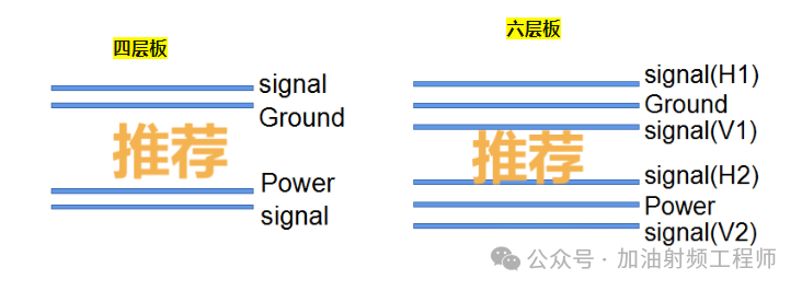
Maybe someone will say, why is one called Ground and the other called Power? Personally, the so-called power plane, when in DC, is the power plane, but when in AC, it can be used as the reference plane of the signal. Just like when you look at microstrip lines, you don't really care about the DC potential of the underlying metal. However, when I do RF layout, the RF signal is generally below the ground plane, that is, the DC potential is 0, although it doesn't matter if the DC potential is not 0, I still tend to avoid it if I can. Moreover, because the current of radio frequency devices is generally not large, as long as the line width is enough, many power supplies are pulled in the past, so it can be completely avoided.
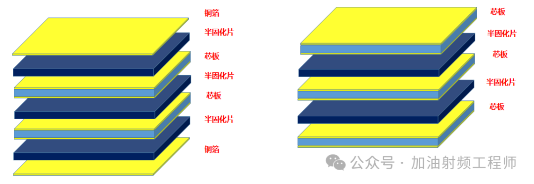
2. Composition of multilayer PCB boardMultilayer PCB is mainly composed of core, prepreg and copper foil. The core board has a medium in the middle and copper foil on both sides, just like a double-layer board. Semi-cured sheets, excluding copper foil, have two main functions: one is glue used for laminating, which is used to stick the upper and lower boards, and the other is used as a dielectric layer after curing. As shown in the figure below, although they are all 6-layer boards with 6 layers of copper, the upper and lower layers on the left are PP and the upper and lower layers on the right are core. In this case, the diagram on the left only needs two core, while the diagram on the right needs three.
We can look at the 6-layer laminated structure given on JLC official website, and you will find that the structure on the left is basically the same, and the upper and lower parts are semi-cured sheets, so that one core plate can be used less. I have never checked the prices of core and PP, and it is said that such costs will be lower.
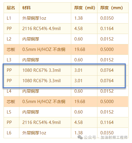
So, it is also 6 floors, which structure should we choose? I think, if the frequency is relatively high, such as C-band or above, it is best to choose the core plate, and the dielectric constant and thickness are guaranteed; PP, sometimes in order to achieve the required thickness, several PP may be stacked together, which increases the uncertainty of thickness and dielectric constant.
3. Why do the TOP layer and the BOTTOM layer need reference planes?Mainly because of backflow. When the signal is transmitted through the microstrip line, it is not only necessary to see the trace of the TOP layer, but also to see the backflow of the corresponding reference plane, so as to form a complete signal transmission. That is to say, when the signal is transmitted on the microstrip line, it needs a reference plane to go back. Why does reflow form in adjacent layers? We can try to understand it separately from the circuit and the field. First, look at the road. exist
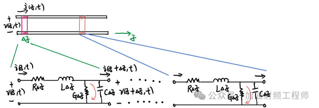
Therefore, when the RF signal is transmitted along the transmission line, there is a voltage difference between the two conductors of the transmission line, thus generating current, and part of it passes through the parallel devices to the reference plane; Part of it continues to walk to the back. That is, a large amount of current will flow on the reference plane below the microstrip line. Now, let's look at it from the perspective of the field. When the signal is transmitted on the microstrip line, it is assumed that the metal is an ideal PEC, and its field distribution and boundary conditions at PEC are shown in the following figure.
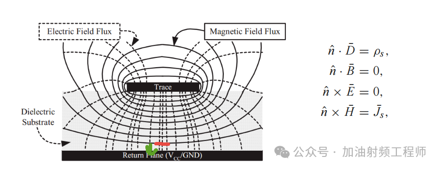
It can be seen that the tangential direction of the magnetic field and the normal direction of the electric field are not zero, so there will be current and charge at the reference plane below the microstrip line.
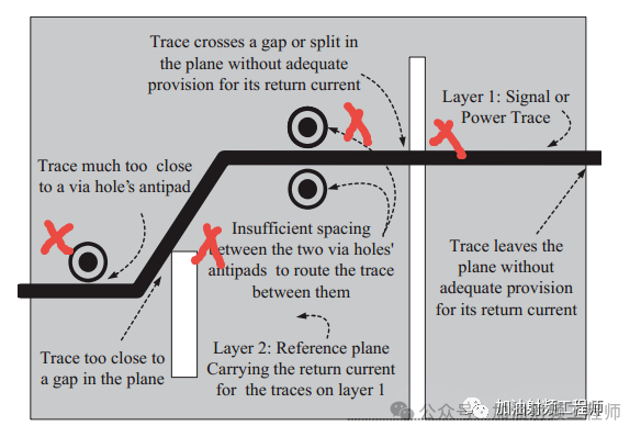
4. What are the requirements for the reference plane below the microstrip line?Mainly, there should be no gaps or too close vias in the reference plane below the microstrip line.
 About Maxipcb
Maxipcb empowers innovators to turn cutting-edge technologies into reality.
We offer one-stop solutions for design, simulation, testing, PCB manufacturing, component procurement and SMT assembly, enabling efficient development, rapid deployment and risk control across the full product lifecycle.Serving the world in communications, industrial automation, aerospace, automotive, semiconductor and beyond, we build a safer, more connected future together. 


