Board-level engineers, especially RF board-level engineers, often have to design PCBs themselves. So what should we consider before starting PCB layout?
Board-level engineers, especially RF board-level engineers, often have to design PCBs themselves. So what should we consider before starting PCB layout?
1. PCB Layer Stackup
A long time ago, RF engineers barely needed to think about stackup design. Why? Because nearly all designs used double‑layer boards: top for routing, bottom as ground, then enclosed in a metal case. As long as the right material was chosen, performance was guaranteed. But double‑layer boards wasted space and cost, so multilayer boards gradually became popular.
With multilayer boards, layer assignment becomes critical. It’s like moving from bungalows to high‑rise buildings—you need to plan which floor to use.
- For pure RF circuits: 4–6 layers are usually sufficient.
- For mixed RF + digital circuits: layer count depends mainly on digital hardware requirements.
For RF circuits, the reference plane under the RF path is the most important. RF components are usually placed on the TOP and BOTTOM layers, so the layers immediately adjacent to TOP and BOTTOM should be reference planes, as shown in the figure below.
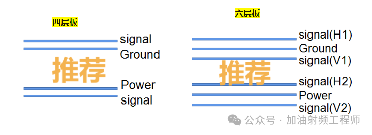
RF PCB stackup with TOP/BOTTOM reference planes (Ground/Power)
Some may ask: why one is called Ground and the other Power?
In my understanding, a power plane acts as a power plane at DC, but as a
signal reference plane at AC. When looking at a microstrip line, we don’t care about the DC potential of the bottom metal.
In RF layout, I prefer to place RF signals over a ground plane (0V DC). Even though non‑zero DC is acceptable, I avoid it when possible. RF current is usually small; as long as trace width is sufficient, power traces can be routed around.
2. Structure of Multilayer PCBs
A multilayer PCB mainly consists of core, prepreg (PP), and copper foil.
- Core: dielectric in the middle, copper on both sides (like a double‑layer board).
- Prepreg: no copper; acts as adhesive during lamination and as dielectric after curing.
As shown in the figure below, both are 6‑layer boards with 6 copper layers, but:
- Left: top/bottom are PP layers; uses only 2 cores.
- Right: top/bottom are core layers; uses 3 cores.
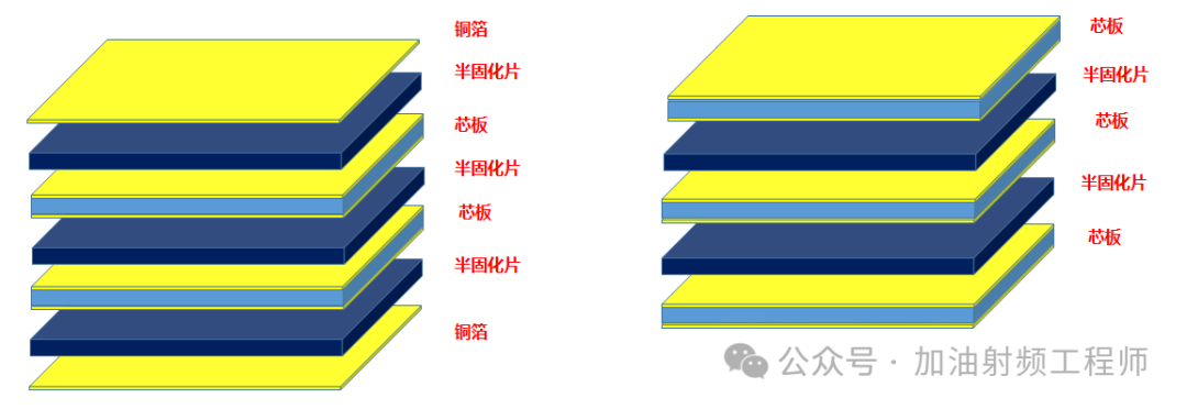
Two 6‑layer PCB stackup structures (core vs. PP)
MaxiPCB’s standard 6‑layer stackup mostly uses the left structure (top/bottom PP) to save one core. I haven’t verified core vs. PP pricing, but this structure is said to lower cost.
Which 6‑layer structure should you choose?
- For high frequencies (above C‑band): prefer core — dielectric constant and thickness are well‑controlled.
- Using PP may require stacking multiple sheets to reach target thickness, increasing uncertainty in thickness and dielectric constant.
3. Why Do TOP and BOTTOM Layers Need Reference Planes?
The main reason is
return current.
When a signal travels along a microstrip line, you must consider not just the TOP trace but also the return current on the reference plane. A complete signal path requires
forward and return currents.
Why does return current form on the adjacent layer? We can explain from circuit theory and field theory.
From circuit theory
The solution to the telegraphers’ equations is the origin of many RF formulas. When the signal wavelength is comparable to the transmission line length, we model a tiny segment of the line using telegraphers’ equations, as shown below.
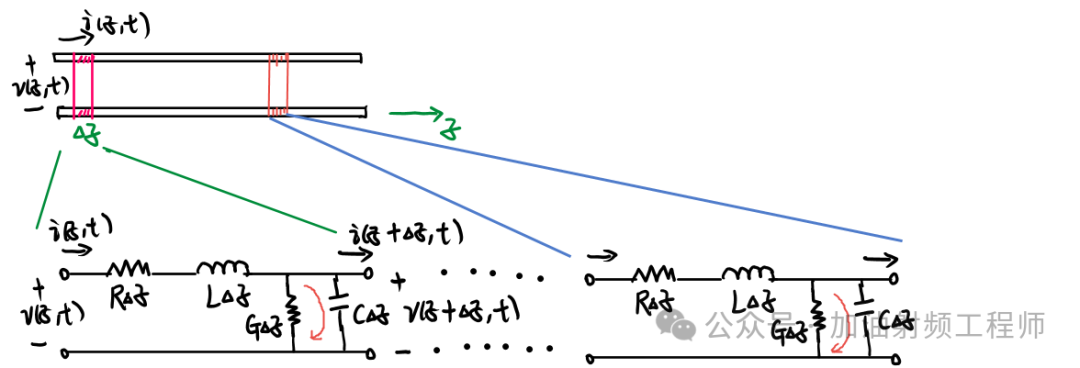
Telegraphers’ equations model for transmission line
As an RF signal travels along the transmission line, voltage difference between the two conductors creates current. Part of the current flows through parallel components to the reference plane; the rest continues forward.
In short,
strong return current flows on the reference plane directly under the microstrip line.
From field theory
Assuming ideal PEC metal, the field distribution and boundary conditions at PEC are shown below.
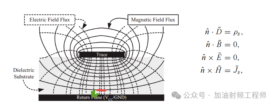
Field distribution around microstrip line
The tangential magnetic field and normal electric field are non‑zero, so current and charge exist on the reference plane under the microstrip line.
4. Requirements for the Reference Plane Under a Microstrip Line
The key rule:
No gaps or closely spaced vias in the reference plane directly under the microstrip line.
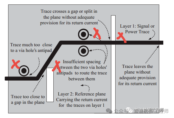
Good vs. bad reference plane under microstrip line
About Maxipcb
Maxipcb empowers innovators to turn cutting-edge technologies into reality.
We offer one-stop solutions for design, simulation, testing, PCB manufacturing, component procurement and SMT assembly, enabling efficient development, rapid deployment and risk control across the full product lifecycle.Serving the world in communications, industrial automation, aerospace, automotive, semiconductor and beyond, we build a safer, more connected future together.


 Field distribution around microstrip line