In today's era of the Internet of Everything, with the continuous development of digitalization, high-level and multi-layer has become the key trend of the future development of PCB industry.
In today's era of the Internet of Everything, with the continuous development of digitalization, high-level and multi-layer has become the key trend of the future development of PCB industry. From a technical point of view, with the advent of 5G and AI era, the demand for PCB in computer and server fields has evolved from high frequency and high speed to stable performance and more complex functions, which undoubtedly puts forward higher requirements for PCB layer number and structure. From the perspective of industrial development, in order to meet the future market demand of communication, intelligent driving and consumer electronics, PCB industry is tending to be high-precision, high-density and high-reliability. Taking the field of automotive electronics as an example, the high-density wiring and reliability of high-layer PCB just meet the requirements of miniaturization, high reliability and environmental adaptability of automotive electronics, so it is widely used in in-vehicle entertainment systems, driver assistance systems, engine control units and safety systems.
High multilayer board not only increases the number of layers, but also increases its manufacturing difficulty exponentially. Today, Aaron takes everyone to master the basic knowledge of high-rise and multi-layer PCB, manufacturing process and process difficulties.
01. Understanding of high-rise and multi-layer plates1, a good high multilayer PCB, board is the key.You may have seen problematic LED light boards in restaurants, banks and other places, either not displaying information or flashing frequently. Why is there a problem with the LED light board? One of the reasons may be that the quality of the PCB used is problematic. As the foundation of PCB products, sheet is not only the core raw material, but also accounts for about 60% of PCB cost. Thus, the importance of plate is self-evident. It is said that good ingredients can make good food. A good board can guarantee a good board. Therefore, it is the key to make PCB and choose the right plate.
Compared with single-layer or double-layer PCB, high-layer PCB faces higher complexity and performance challenges. This is mainly reflected in three aspects:
The first is the transmission characteristics of high-frequency signals. High-multilayer PCB is often used in applications that need high-frequency signal transmission, such as communication equipment and high-speed digital signal processing. This requires PCB to have better dielectric performance and signal transmission speed to reduce signal loss and noise.
The second is the demand for thermal management. High-multilayer PCB is usually used in high-power electronic equipment, and effective thermal management measures are needed to ensure the normal working temperature of components. This requires PCB to have better thermal conductivity and thermal expansion coefficient control to optimize heat conduction and distribution and avoid hot spots and thermal stress problems.
The third is the requirement of mechanical strength and stability. High multilayer PCB usually has a larger size and a higher number of layers, so it needs higher mechanical strength and stability. The rigidity and durability of the board are very important to resist vibration, impact and bending stress, so as to ensure the reliability and life of high-multilayer PCB.
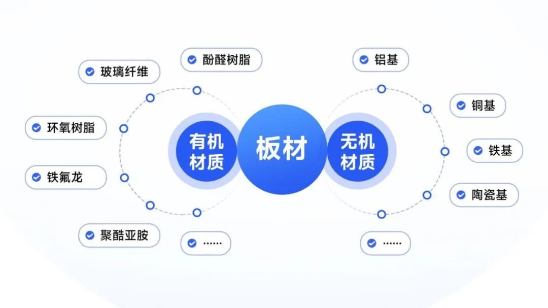
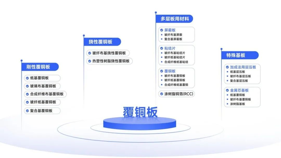
2, the classification of high multilayer PCB boardCCL-Copper Clad Laminate, also known as CORE in PCB multilayer production, is the key raw material of high multilayer PCB. It is composed of copper foil, resin, glass fiber cloth and other functional reinforcing additives. By dipping the reinforcing material into resin, and sticking copper foil on one or both sides, a plate-like material is formed by hot pressing, which is what we call copper-clad laminate. In classification, plates can be distinguished according to different dimensions such as material, hardness, structure and grade of finished products.
Specifically, plates can be divided into two categories: organic materials and inorganic materials.
According to the hardness of the finished product, the board is divided into hard board, soft board and soft-hard combined board. Hard board is the most common type, which is used in most standard electronic equipment; Flexible board has high flexibility and is suitable for application scenes that need bending; The combination of soft and hard board combines the stability of hard board and the flexibility of soft board, which is suitable for complex electronic product design.
Structurally, the board can be divided into single panel, double panel, multi-layer board and HDI (high density interconnection board, characterized by blind hole burying technology). Only one side of a single panel has a conductive path, and circuits are distributed on both sides of a double panel; Multilayer board increases circuit density through multilayer conductive layers; HDI board realizes higher line density and smaller electronic equipment size through blind hole burying technology.
According to the grade of PCB, PCB includes 94HB (lowest flame retardant grade) and 94V0 (higher flame retardant performance). Among them, under 94V0 level, it is subdivided into FR1, 22F, CEM-1, CEM-3 and FR-4. FR1 is mainly used for single panel; 22F is often used for cost-sensitive products; CEM-1 and CEM-3 are suitable for double-panel applications; FR-4 is widely used in the manufacture of multilayer boards because of its excellent electrical insulation, high mechanical strength and good wet-heat stability.
According to the different reinforced materials of the substrate, it can be divided into five categories: paper base, glass fiber cloth base, composite base (CM series), laminated multi-layer board base and special material base (ceramics, metal core base, etc.).
 3, high multilayer PCB plate selection
When placing an order on PCB, you may encounter the situation that the required plates are out of stock. At this time, it is particularly important to choose alternative materials with the same performance grade. The selection of high and multi-layer PCB board is not only influenced by the material itself and internal characteristics, but also includes external factors. Internal factors cover a series of important considerations, such as appearance requirements, size standards, electrical properties, thermal properties and physical (mechanical) properties.
Among them, the appearance requirements, including dents, wrinkles, scratches, bubbles and other defects on the metal foil surface, may affect the quality and performance of the final product. Size requirements involve the length, width, diagonal deviation, warpage and so on. Accurate size is very important to ensure the assembly accuracy and performance of PCB.
Next,
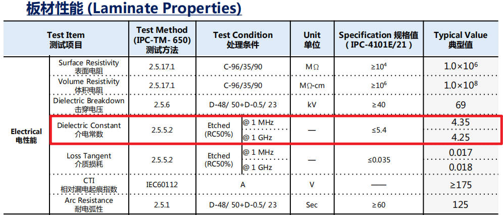
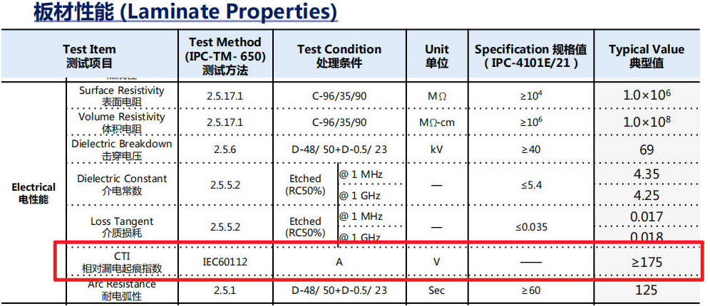
we will focus on the electrical performance, thermal performance and physical (mechanical) performance.behaviour of electricityElectrical properties include dielectric constant (Dk), dielectric loss tangent (DF), volume resistance, surface resistance, insulation resistance, arc resistance, breakdown voltage, electrical strength and relative leakage tracking index (CTI).
Among them, dielectric constant (Dk), dielectric loss tangent (DF) and relative leakage tracking index (CTI) are the electrical performance parameters that users are most concerned about when choosing PCB.
Dielectric constant, that is, Dk, English full name Dielectric constant. It is a physical property that describes the ability of materials to store charge, and has a significant impact on capacitor performance and electric field distribution. Materials with high dielectric constant can store more charges, which is especially important for applications requiring high capacitance performance. In addition, the dielectric constant also determines the propagation speed and concentration degree of electric field in the medium. For example, the dielectric constant of FR4 plate is generally between 4.2 and 4.6, while that of Teflon is between 2.0 and 3.0, and that of green oil is between 3.4 and 3.8.
Product technical data of a manufacturer
The tangent of dielectric loss angle, that is, DF, or loss factor, is an important physical parameter to describe the energy loss of dielectric materials in alternating current field. It reflects the ratio of electric field energy loss to stored energy in materials, which is closely related to the molecular structure, chemical composition and temperature of materials. In the design of electronic devices and circuits, DF is a key parameter, which directly affects the bandwidth, attenuation and phase distortion of signals, especially in high-frequency circuits and communication systems. Choosing a material with low DF value can significantly reduce signal loss and maintain good signal integrity. For example, PTFE, a low-loss material, is generally used as an antenna board.
The relative leakage trace index (CTI) is also very important, which measures the electrical breakdown resistance of insulating materials under the action of electric arc. CTI is a key parameter to evaluate the arc resistance of materials, especially to determine the safety and reliability of materials under specific environmental conditions. The value of CTI is usually expressed by standardized classification. The higher the value, the better the arc performance of the material.
Product technical data of a manufacturer
The value of CTI is directly related to the insulation performance and arc resistance of materials, in which higher CTI value means that materials can maintain their insulation at higher voltage and show better arc resistance. This characteristic is very important for electrical equipment and electronic products, because it ensures that materials can provide adequate protection when arc events occur, thus greatly reducing the risk of fire and other accidents. Therefore, when designing and selecting electronic materials, materials with high CTI value are often given priority to ensure the safety and reliability of the whole system.
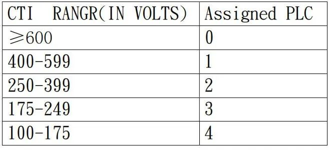
Criterion for judging CTI test grade
Generally, the CTI value is expressed in a standardized classification, in which the higher the value, the better the arc performance of the material. At present, all materials CTI of MaxiPCB are Grade 3, ranging from 175 to 249 V.
hot property
Thermal properties mainly include Tg value, Td value, CTE, thermal stress, combustibility and so on.
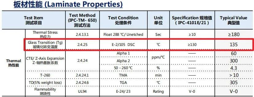
Tg value, also called glass transition temperature, is one of the key indexes to measure the thermal properties of PCB. It marks the critical point that materials (such as PCB) change from hard and brittle glass state to soft rubber state with the increase of temperature. In the field of PCB manufacturing, this glassy substance usually refers to the resin or the mixture of resin and glass fiber cloth that constitutes the dielectric layer.
Product technical data of a manufacturer
Tg value has a great influence on the reliability and performance of PCB. When the PCB works in its operating temperature range, it is very important to keep the material in a glassy state, which can ensure the stability of the mechanical and electrical properties of the PCB. If the PCB exceeds its Tg value in use, the board may become soft, which may lead to the decrease of dimensional stability, and may even affect the integrity of wires and solder joints, thus reducing the performance and reliability of the whole circuit board.
The Tg requirement of common sheet is greater than 135℃, the medium Tg requirement is greater than 150℃, and the high Tg requirement is greater than 170℃. The higher the Tg, the better the heat resistance and dimensional stability of the plate.
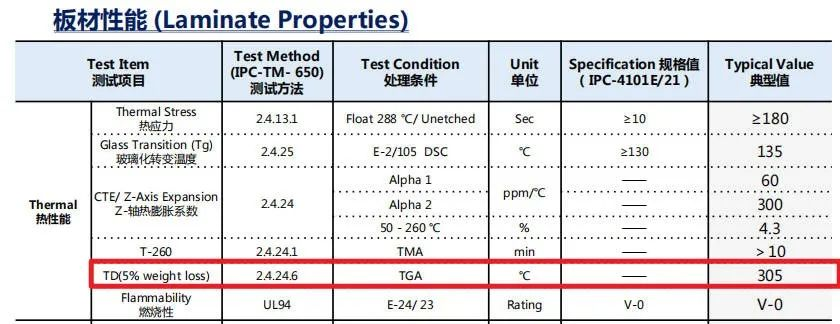
Td value, that is, thermal decomposition temperature. It refers to the temperature at which chemical decomposition of materials begins at high temperature. This is an important index to measure the thermal stability and high temperature resistance of plates in high temperature environment. In electronic equipment working under high power or high temperature conditions, if PCB has a high Td value, it means that it can better withstand these conditions without decomposition or loss of performance, and ensure the long-term stable operation of the circuit.
Product technical data of a manufacturer
The higher the Td value, the higher the temperature and thermal stress can be, and the normal function of the circuit can be maintained and the service life of the equipment can be prolonged.
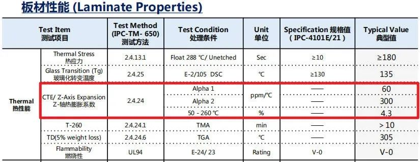
CTE, the Coefficient of Thermal Expansion, is the full name of coefficient of thermal expansion in English. It is used to describe the dimensional change of PCB under the temperature change. Every time the temperature rises by one degree, the material will expand or contract when it cools. Because PCB is usually composed of resin, copper foil and glass fiber reinforced materials, the CTE values of these materials are different, which leads to their different expansion or contraction speeds when the temperature changes. This mismatched thermal expansion behavior may cause dimensional instability, stress concentration, and even problems in subsequent processing such as welding.
Product technical data of a manufacturer
The lower the CTE value, the better the dimensional stability, and vice versa.
Physical (mechanical) performance
In terms of physical and mechanical properties, the quality and applicability of PCB are affected by many factors, including peeling strength, bending strength, water absorption and flammability of copper foil.
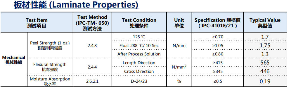
In addition, CAF is also particularly important. CAF phenomenon, also known as wick effect, is called Conductive Anodic Filament. It means that under the conditions of high temperature, high humidity, high pressure, etc., after long-term use of the product, the glass fiber of the plate is used as a channel, which leads to the growth of copper foil on the hole wall and the formation of slender conductive filaments, which may eventually form short circuits or short circuits between adjacent holes. Even more difficult, when PCB products are baked again, this kind of fault may disappear temporarily, making it difficult to identify and solve the problem immediately. There are many reasons for CAF, including materials, drilling, electroplating and data design (the hole spacing is less than IPC2 level 2 standard).
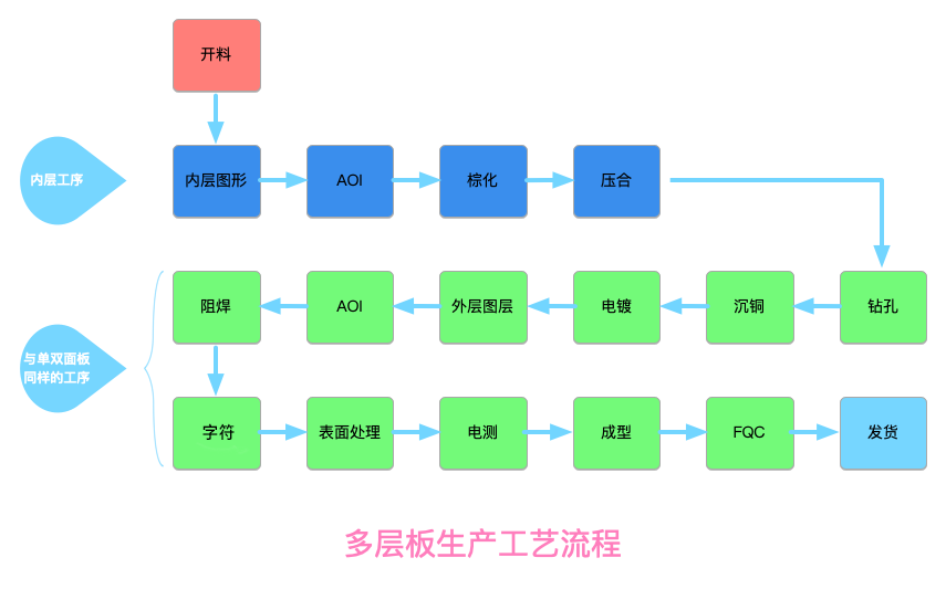
02. Manufacturing process of high multilayer PCBFirst, let's look at the picture.
The following figure shows the production process flow of multilayer board. Compared with the manufacturing of single and double-sided PCB, the manufacturing of multilayer board has an inner layer process flow, and the key step is the control of the lamination process of inner layer, which is very important for the electrical performance of controlled impedance transmission line. After the lamination of the inner layer process is completed, it comes to the same manufacturing process as the single and double panels, until the final inspection process.
Let's take a step-by-step look at the key steps of high-level and multi-layer PCB manufacturing.
1. Submit manufacturing informationAs the beginning of PCB manufacturing, first of all, we need to submit relevant manufacturing information to PCB factory. Information and common data formats required for PCB manufacturing include the following:
Gerber file (RS274X format)
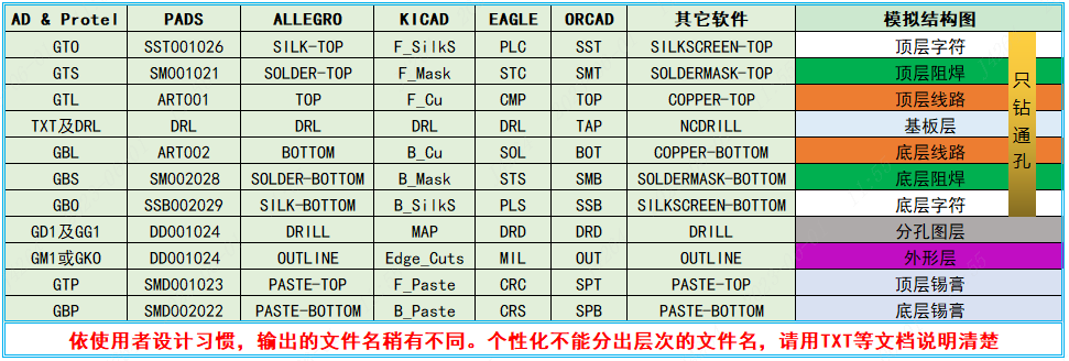
Gerber RS274X is the mainstream format at present, and the output Gerber file includes all circuit layers, solder resist layers, solder paste layers, screen printing (character) layers, plate frames, hole diagrams, and manufacturing requirements (such as schematic diagram of multilayer laminated structure, interlayer dielectric thickness, impedance control requirements, hole plugging requirements, etc.). At the same time, Gerber files should be convenient for process engineers in PCB factory to identify the layer information corresponding to each Gerber file, so it is recommended to name Gerber files according to a certain naming convention. For example, this naming specification given by MaxiPCB is a good reference:
 Drilling file
Drilling file contains all drilling coordinates and diameter data, and the common file format is Excellon format.
Net table dataIPC defines the compatible format IPC-356, which provides all necessary information for generating netlist and electrical performance test data. Compared with single-layer or double-panel, a complete PCB document is very important for the manufacturing of multi-layer PCB. The most important information in the manufacturing information document is:
Complete layer structure
Accurate information about the substrate
High-frequency and high-speed plates also need to provide the base material manufacturer and product name.
Impedance control requirements
Special process instructions (such as plug hole requirements)
2. Manufacturing information auditThe purpose of auditing manufacturing information by PCB factory is to determine the approximate manufacturing cost and prepare for manufacturing. Before the product is manufactured or processed, proper preliminary analysis can save time and materials. The responsibility of PCB factory is to determine whether its technological capacity can meet the given product.
PCB factory will adjust the wiring information of PCB design according to its manufacturing process, such as compensation for via drilling diameter or compensation for routing etching, in order to improve the manufacturability of PCB. Some key modifications will also be communicated with PCB Layout for confirmation. Of course, it is ideal to consider DFM manufacturability and optimize the design during the process of PCB design, which will save a lot of time for communication and confirmation with PCB factory in the later period.
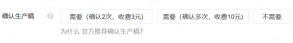
If you are playing in MaxiPCB, their family also provides a personalized service of "confirming the production draft". As long as we carefully check and confirm, we can find out the problems in our design, and of course we can also find some mistakes in the processing of MaxiPCB engineers. If it's MaxiPCB's problem, don't forget to ask the engineering staff to return the cost of confirming the production draft.
 3. Material selection
In the first part, we introduced the high and multi-layer PCB board in detail, so I won't expand it here.
4. Manufacturing process of multilayer boardIf the production process of multilayer board is developed in detail, it usually needs about 200 different processing steps. Therefore, it is very important for PCB designers to be familiar with the different types and properties of substrates, the manufacturing process of multilayer boards and the welding process. By combining prepreg and copper-clad laminate (core board) with different specifications, all required thicknesses can be achieved. For the laminated structure of multi-layer board, it should be noted that each layer structure must be symmetrical and have the same layer thickness. The copper in the inner layer should be evenly distributed on these symmetrical layers. If the distribution is uneven, the uneven thermal stress during heating will cause the circuit board to warp.
One of the factors that have a great influence on the quality of multilayer structure is the precise adjustment between layers. These layers must be exactly overlapped, otherwise the circuit between the layers may be open and short after being connected by drilling. The alignment holes are precisely adjusted by machinery, and then the positioning pins are used to adjust the lamination. In order to ensure good adhesion between the inner layer and the prepreg, the copper surface must be chemically roughened, which is called browning. Before laminating multilayer printed circuit boards, it is very important to inspect the internal circuit layers to ensure the quality. At this stage, if the inspection finds connection or other defects, it can still be repaired. The inspection is usually carried out automatically by AOI (Automatic Optical Inspection), and the AOI system directly compares the etched circuit patterns with CAD data.
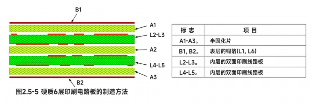
The above picture is a schematic diagram of the manufacturing of 6-layer rigid multi-layer board by pressing. A1, A2 and A3 are semi-cured sheets, L2-L3 and L4-L5 are double-sided copper-clad laminates that complete the inner layer pattern, and B1 and B2 are copper foils for the outer layer circuit.
The conventional lamination principle of rigid multilayer board is to combine a certain number of double-sided copper clad plates (the inner layer pattern has been completed and browned to strengthen the bonding force), and the double-sided copper clad plates are separated by prepreg, which is used as insulating material to avoid short circuit of each copper layer, and at the same time, after the prepreg is heated, the resin in it will be melted again to realize the bonding of each copper clad laminate. Finally, the laminated layers are connected through metallized holes. At present, MaxiPCB's multi-layer board manufacturing process can manufacture up to 32 layers of multi-layer boards, which is enough to cover most application scenarios.
Precise control of pressing is very important for the characteristic impedance of controlled impedance transmission lines. During pressing, with the increase of temperature, the epoxy resin in the prepreg will melt again, and it will fill the gap between the wires by flowing, and bond the inner layers together. The flowing property of the resin will affect the distance between the final signal layer and the reference layer, and the change of the distance between the signal layer and its reference layer has the greatest influence on the impedance change.
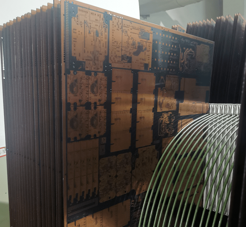
As shown in the above figure, the design draft of PCB is finally assembled on a large working panel for production. For the control of characteristic impedance, the influence of resin flow uniformity on impedance change can not be ignored when the whole large panel is pressed, and the performance of the pressing equipment used at this time is also very important.
03. Key technology of high multilayer PCBIn the manufacture of high-rise multilayer board, a good PCB and board are the key. However, the process is directly related to the quality of high-level and multi-layer PCB. Speaking of this, MaxiPCB is a professional manufacturer who has been deeply involved in PCB industry for nearly 20 years. In the production of high-level multilayer boards, MaxiPCB adopts gold sinking technology, middle hole technology and positive film technology to ensure the high quality of products in all directions.
MaxiPCB's 6-32-layer circuit boards all adopt gold sinking technology, and the thickness of gold sinking is upgraded to 2u "for free. Gold deposition is a relatively expensive surface treatment method in the industry, which can provide good electrical connection, corrosion resistance and welding performance. The deposited gold layer can provide a smooth and uniform metal surface, which helps to maintain good signal transmission and impedance control. Moreover, it can ensure the stability and durability of the metal layer in the welding process, provide excellent corrosion resistance and prolong the service life of PCB.
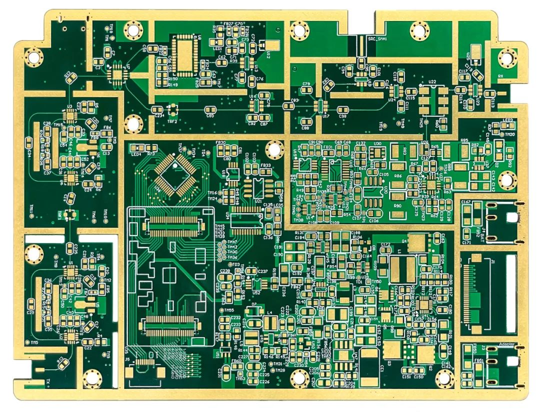
PCB (produced by gold sinking process and middle hole process)
In addition to the gold sinking process, MaxiPCB adopts the middle hole process (resin plug hole+electroplating cap) for 6-32 laminates free of charge. Via is very important for the quality of PCB, because it plays an important role in electronic equipment and supports the realization of complex circuits and the reliability of functions. Due to various factors, vias will be slowly corroded, which will lead to connection failure, signal attenuation, short circuit and leakage, and reliability problems, and the hole-in-plate technology can effectively solve these problems.
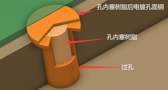
Three-dimensional diagram of hole technology in disc
The hole in the plate is punched in the welding plate. During production, the resin is filled in the hole, dried and ground, and then the surface copper is electroplated. Its advantages are not only greatly improving the efficiency of PCB design engineers, shortening the design time from 7 days to about 2 days, but also greatly improving the yield of PCB and improving the performance of high-speed board.
About Maxipcb
Maxipcb empowers innovators to turn cutting-edge technologies into reality.
We offer one-stop solutions for design, simulation, testing, PCB manufacturing, component procurement and SMT assembly, enabling efficient development, rapid deployment and risk control across the full product lifecycle.Serving the world in communications, industrial automation, aerospace, automotive, semiconductor and beyond, we build a safer, more connected future together. 


