Driven by emerging demands represented by artificial intelligence and high-performance computing, advanced packaging has emerged as the times require, with the development trends of miniaturization and high integration. It has gone through four development stages: through-hole packaging, surface mount technology, area array packaging, 2.5D/3D packaging and heterogeneous integration.
Driven by emerging demands represented by artificial intelligence and high-performance computing, advanced packaging has emerged as the times require, with the development trends of miniaturization and high integration. It has gone through four development stages: through-hole packaging, surface mount technology, area array packaging, 2.5D/3D packaging and heterogeneous integration.
Advanced packaging has pioneered the More-than-Moore development route for integrated circuits. It can improve chip performance only by optimizing the packaging method without shrinking the process node, and also break through the "memory wall" and "area wall".
Also known as high-density packaging, advanced packaging features a large number of pins, a compact chip system and high integration. It belongs to the middle-end process, including a series of steps such as cleaning, sputtering, photoresist coating, exposure, development, electroplating, photoresist stripping, etching, solder flux coating, reflow soldering, cleaning and testing. Different from the traditional back-end packaging and testing processes, the key processes of advanced packaging need to be completed on the front-end platform and are an extension of the front-end processes.
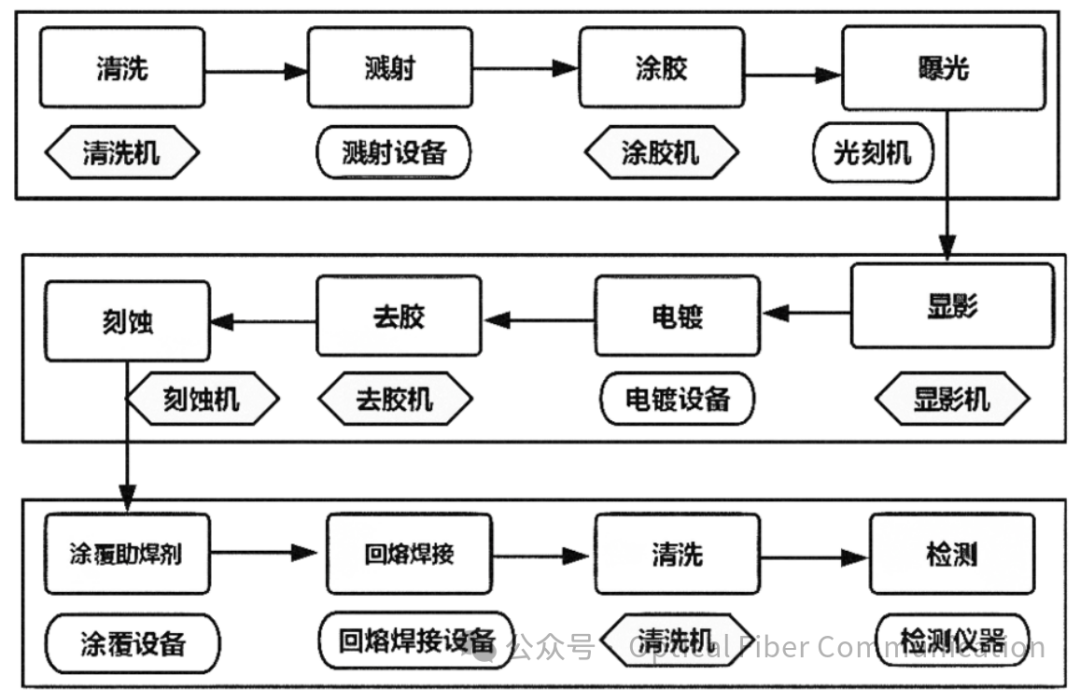
| Process |
Corresponding Equipment |
| Cleaning, Sputtering, Photoresist Coating, Exposure |
Cleaning Machine, Sputtering Equipment, Photoresist Coater, Lithography Machine |
| Etching, Photoresist Stripping, Electroplating, Development |
Etching Machine, Photoresist Stripper, Electroplating Equipment, Developer |
| Solder Flux Coating, Reflow Soldering, Cleaning, Testing |
Coating Equipment, Reflow Soldering Equipment, Cleaning Machine, Testing Instrument |
Now let's briefly understand several advanced packaging technologies.
1. FOWLP
FOWLP (Fan-out Wafer Level Package) is a type of WLP (Wafer Level Package), so we first need to understand wafer level packaging. Wafer level packaging can be divided into two main types: Fan-In WLCSP (Fan-In Wafer Level Chip Scale Package) and Fan-Out WLCSP (Fan-Out Wafer Level Chip Scale Package).
Traditional Packaging vs Wafer Level Packaging
Traditional packaging processes follow the sequence of
wafer → dicing → packaging, while wafer level packaging follows
wafer → packaging → dicing.
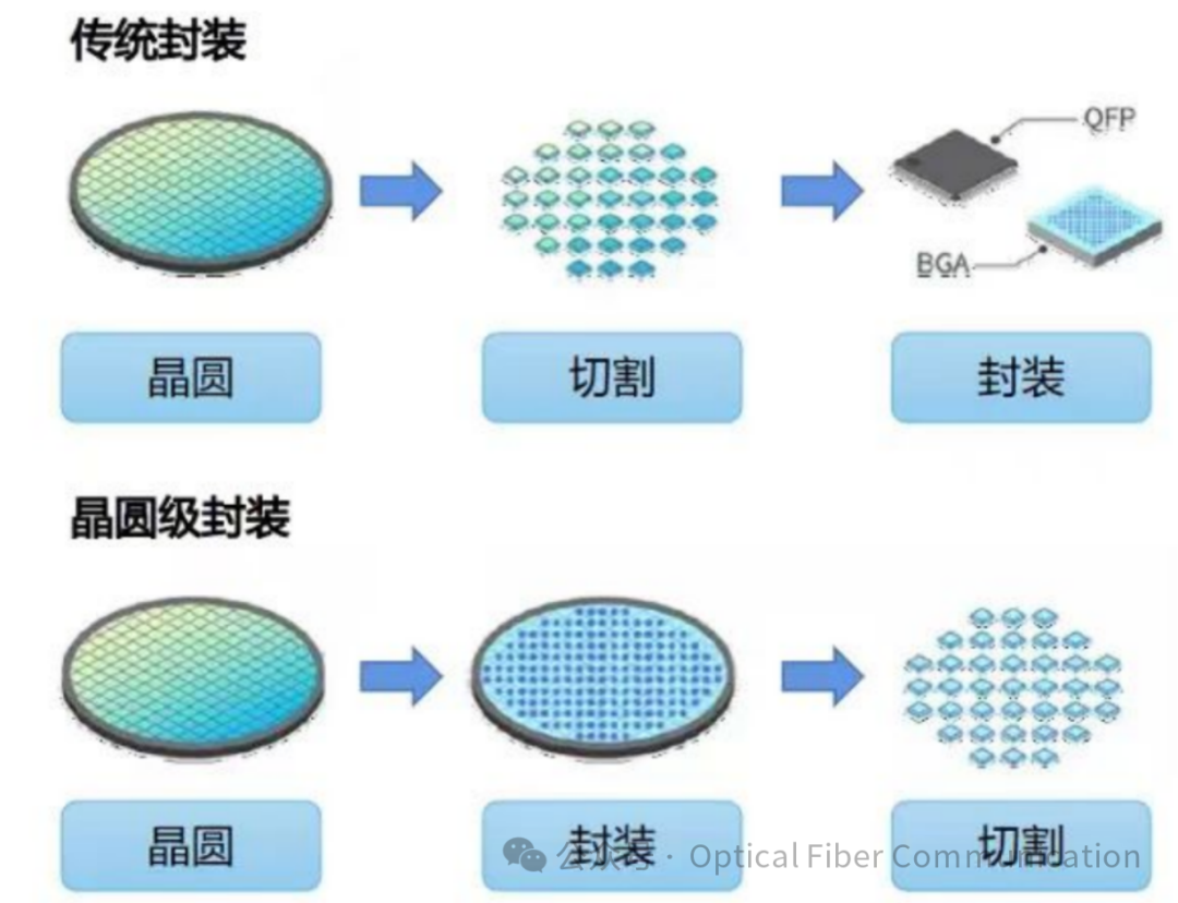
Since dicing and singulation are carried out after packaging is completed, the size of the packaged chip is almost the same as that of the bare die. Therefore, it is also called CSP (Chip Scale Package) or WLCSP (Wafer Level Chip Scale Packaging). This type of packaging conforms to the market trend of light, small, short and thin consumer electronic products, with low parasitic capacitance and inductance, as well as advantages such as low cost and excellent heat dissipation.
For FOWLP, since RDL and Bump need to be led out to the periphery of the bare die, it is necessary to first dice and separate the bare die wafer, then reconfigure the independent bare dies into the wafer process, and on this basis, form the final package through batch processing and metallization wiring interconnection.
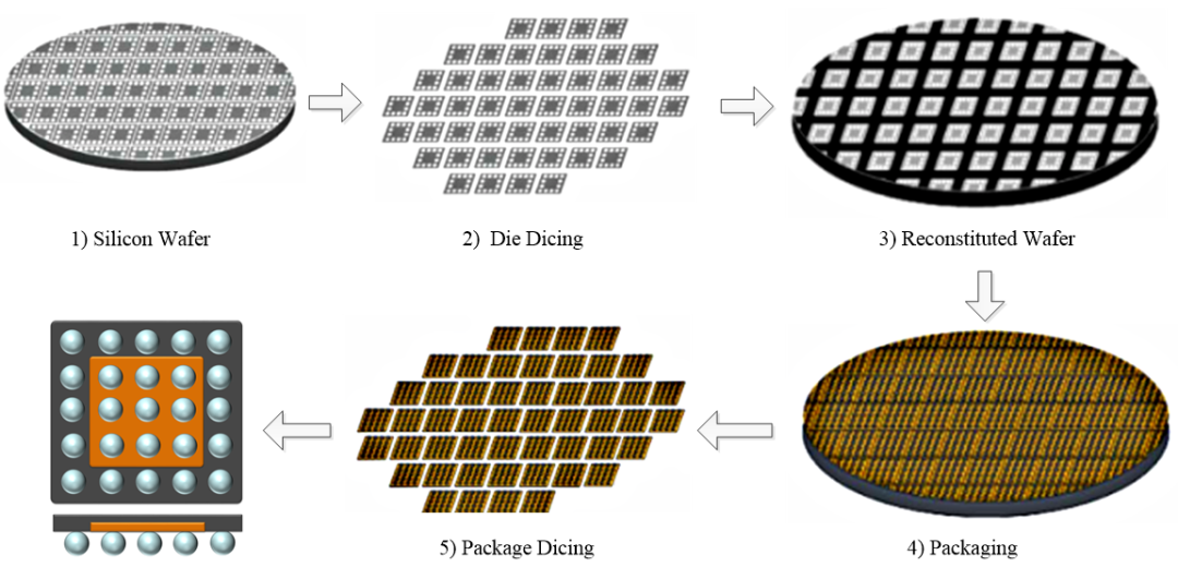
FOWLP packaging process steps:
- Silicon Wafer
- Die Dicing
- Reconstituted Wafer
- Packaging
- Package Dicing
Whether Fan-in or Fan-out is adopted, the connection between WLP wafer level packaging and PCB is realized in flip-chip form, with the active side of the chip facing down towards the printed circuit board. This achieves the shortest circuit path, which also ensures higher speed and fewer parasitic effects. On the other hand, due to the adoption of batch packaging, the entire wafer can be packaged at one time, and cost reduction is another driving force for wafer level packaging.
FOPLP
FOPLP adopts the production technology on PCB for RDL production, with its line width and line spacing both greater than 10um at present. SMT equipment is used for the mounting of chips and passive components. Since the panel area is much larger than the wafer area, more products can be packaged at one time. Compared with FOWLP, FOPLP has a greater cost advantage. At present, major global packaging manufacturers including Samsung Electronics and ASE Group are actively investing in FOPLP process technology.
2. EMIB
EMIB (Embedded Multi-Die Interconnect Bridge) is an advanced packaging technology proposed and actively applied by Intel. Different from the three advanced packaging technologies described above, EMIB is a substrate-based packaging technology, and because it does not have TSV, it is also classified as an advanced packaging technology extended based on the XY plane.
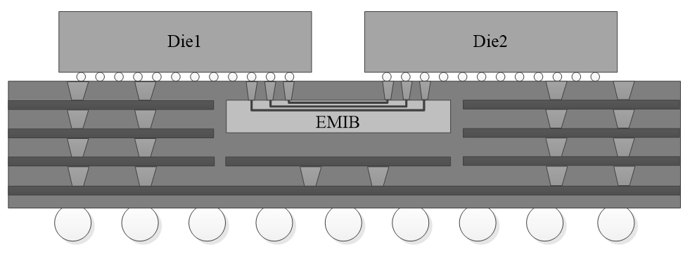
Compared with the silicon interposer, the EMIB silicon chip has a smaller area, higher flexibility and better economy. EMIB packaging technology can package CPU, IO, GPU and even FPGA, AI chips together as needed, and can package chips with various processes such as 10nm, 14nm and 22nm into a single chip to adapt to flexible business needs.
Through the EMIB method, the KBL-G platform integrates Intel Core processor with AMD Radeon RX Vega M GPU, which not only has the powerful computing power of Intel processor and the excellent graphics performance of AMD GPU, but also provides an excellent heat dissipation experience. This chip has created history and raised the product experience to a new level.
3. CoWoS
The high-density connection and short interconnection pitch of HBM call for TSMC's CoWoS packaging technology, which is a 2.5D packaging technology. CoWoS is a 2.5D integrated packaging technology developed by TSMC in 2012, which can be divided into two steps: CoW and oS. CoW (chip on wafer) is to package computing cores, I/O die, HBM and other chips on the silicon interposer; then the entire CoW chip is packaged on the substrate, which is the oS (on substrate) step.
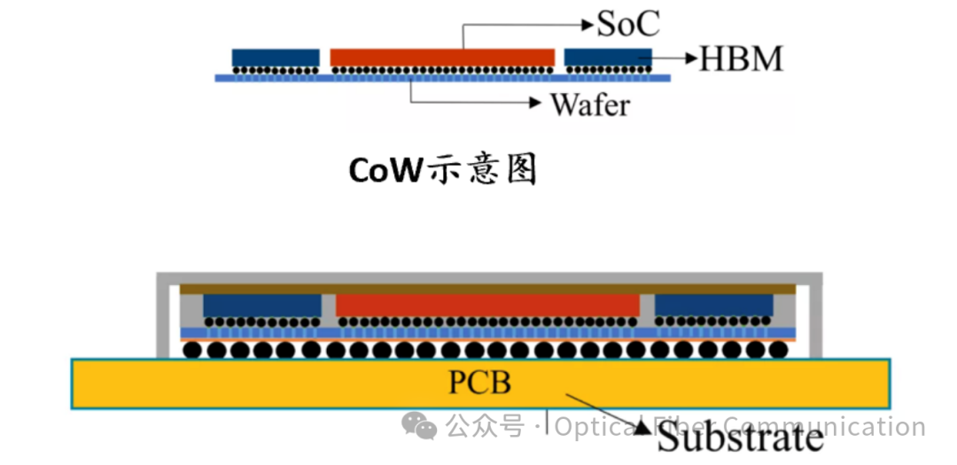
CoWoS can save space, achieve the high interconnection density and short-distance connection required by HBM; it can also package chips with different processes together, meeting the needs of accelerated computing such as AI and GPU while controlling costs. At present, all advanced AI computing chips use HBM, and almost all HBM are packaged on CoWoS.
4. HBM
HBM (High-Bandwidth Memory) is mainly targeted at the high-end graphics card market. HBM adopts 3D TSV and 2.5D TSV technologies, stacking multiple memory chips together through 3D TSV, and realizing the interconnection between stacked memory chips and GPU on the substrate by using 2.5D TSV technology.
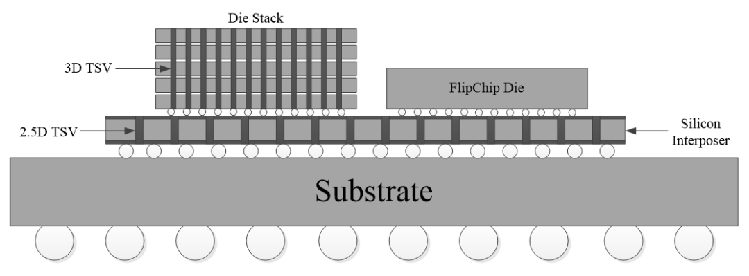
HBM structure composition: Die Stack, 3D TSV, FlipChip Die, 2.5D TSV Interposer Silicon, Substrate
At present, there are three versions of HBM, namely HBM, HBM2 and HBM2E, with bandwidths of 128 GBps/Stack, 256 GBps/Stack and 307 GBps/Stack respectively, and the latest HBM3 is still under development.
5. SoIC
SoIC, also known as TSMC-SoIC, is a new technology—System-on-Integrated-Chips, which TSMC expected to put into mass production in 2021. What exactly is SoIC? It is an innovative multi-chip stacking technology that can realize wafer-level integration for processes below 10 nanometers. The most distinctive feature of this technology is its bump-free bonding structure, thus having higher integration density and better operating performance.
SoIC includes two technical forms: CoW (Chip-on-wafer) and WoW (Wafer-on-wafer). According to TSMC's description, SoIC is a direct bonding technology for WoW wafer-on-wafer or CoW chip-on-wafer, belonging to Front-End 3D technology (FE 3D), while the aforementioned InFO and CoWoS belong to Back-End 3D technology (BE 3D). TSMC has cooperated with Siemens EDA (Mentor) on SoIC technology and launched relevant design and verification tools.
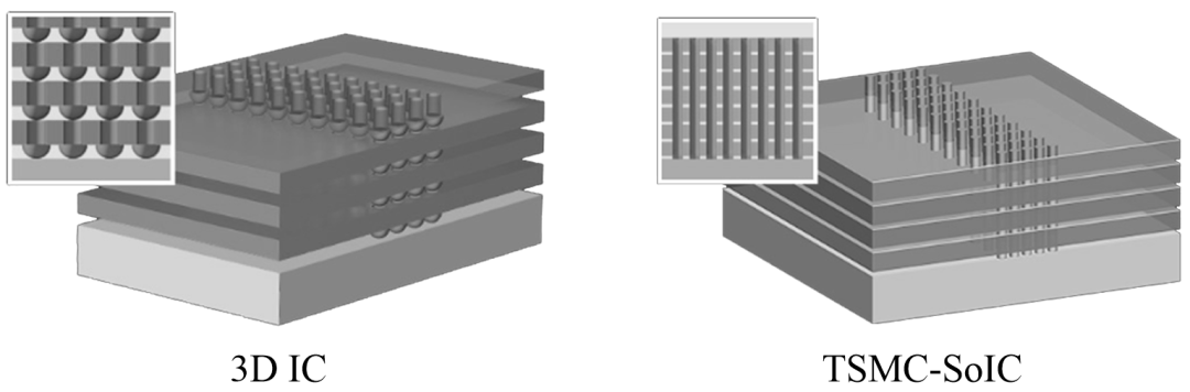
Specifically, the manufacturing process of SoIC is somewhat similar to that of 3D IC. The key of SoIC is to realize a bump-free bonding structure, and its TSV density is also higher than that of traditional 3D IC, realizing the interconnection between multi-layer chips directly through extremely tiny TSV. It can be seen from the figure that the TSV density of SoIC is much higher than that of 3D IC, and at the same time, the interconnection between chips adopts bump-free direct bonding technology, resulting in a smaller chip pitch and higher integration density, thus its products have higher functional density than traditional 3D IC.
6. X-Cube
X-Cube (eXtended-Cube) is a 3D integration technology that can accommodate more memory in a smaller space and shorten the signal distance between units. X-Cube is used in processes requiring high performance and bandwidth, such as 5G, artificial intelligence, wearable or mobile devices, and applications requiring high computing power.
X-Cube uses TSV technology to stack SRAM on top of logic units, which can accommodate more memory in a smaller space.
It can be seen from the X-Cube technology display diagram that different from the previous 2D parallel packaging of multiple chips, X-Cube 3D packaging allows stacked packaging of multiple chips, making the finished chip structure more compact. The chips are connected by TSV technology, which reduces power consumption while improving transmission speed. This technology will be applied in the cutting-edge fields such as 5G, AI, AR, HPC, mobile chips and VR.
X-Cube technology greatly shortens the signal transmission distance between chips, improves data transmission speed, reduces power consumption, and can customize memory bandwidth and density according to customer needs. At present, X-Cube technology can support 7nm and 5nm processes, and Samsung will continue to cooperate with global semiconductor companies to deploy this technology in a new generation of high-performance chips.
The Improvement Effects of Advanced Packaging on Chips
Advanced packaging improves chips in five aspects:
- Realize miniaturization, high density and multi-function of chip packaging;
- Reduce product power consumption, improve product bandwidth and reduce signal transmission delay;
- Realize heterogeneous and heterostructured system integration;
- An effective way to continue Moore's Law and improve product performance;
- Reduce the design complexity and manufacturing cost of advanced node chips, shorten the development cycle and improve product yield.
About Maxipcb
Maxipcb empowers innovators to turn cutting-edge technologies into reality.
We offer one-stop solutions for design, simulation, testing, PCB manufacturing, component procurement and SMT assembly, enabling efficient development, rapid deployment and risk control across the full product lifecycle.Serving the world in communications, industrial automation, aerospace, automotive, semiconductor and beyond, we build a safer, more connected future together.


 FOWLP packaging process steps:

 HBM structure composition: Die Stack, 3D TSV, FlipChip Die, 2.5D TSV Interposer Silicon, Substrate