PCB impedance is a combination of capacitance and inductance of a circuit during high-frequency operation. Although it is also measured in ohms (Ω), it differs from resistance, which is a DC characteristic. Impedance is an AC characteristic, meaning it is related to frequency, while resistance is not.
What is PCB Impedance?
PCB impedance is a combination of capacitance and inductance of a circuit during high-frequency operation. Although it is also measured in ohms (Ω), it differs from resistance, which is a DC characteristic. Impedance is an AC characteristic, meaning it is related to frequency, while resistance is not.
The Significance of Impedance for PCBs
Impedance matching is a necessity for PCBs to achieve high-speed data transmission.
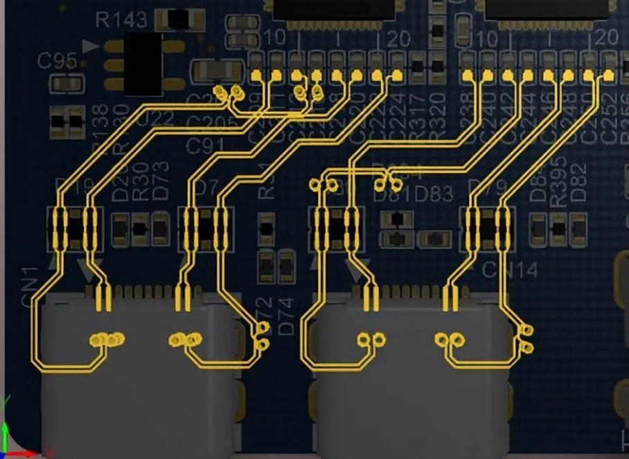
Take the mobile phone USB interface as an example—it enables synchronous data transmission in two directions with high speed and low cost. The common types are Type-A, Type-B and Type-C.
The USB protocol defines differential signal lines (D+, D-), (TX+, TX-), (Rx+, RX-) for transmitting digital signals. To ensure the stability of transmitted signals, the PCB design of differential lines must strictly follow the routing rules for differential signals.
Key Considerations for Multi-layer PCB Impedance Routing
-
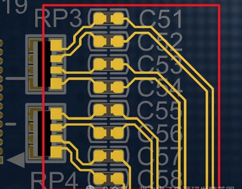
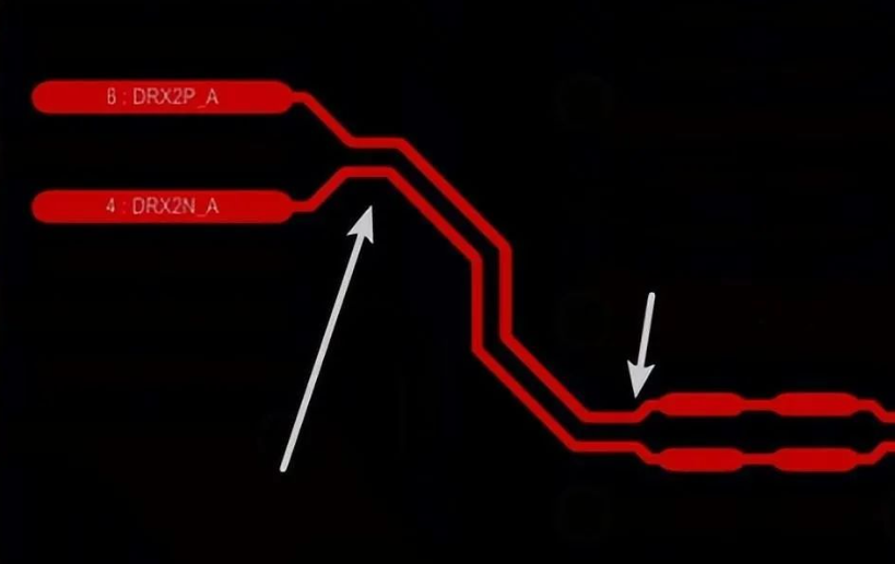
Component pads should be arranged as close as possible to shorten the distance between pads, minimize the length of differential lines, and use as few vias as possible.
-
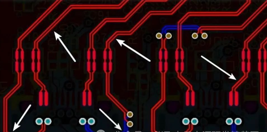
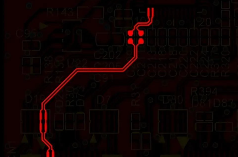
Routes should be parallel and symmetrical. Right-angle (90°) routing is not allowed; 45° or arc routing should be adopted instead. The line spacing should be controlled within 4 mil.
-
When connecting resistors and capacitors in series, they should be aligned vertically or horizontally.
-
Differential impedance lines should be kept as equidistant as possible to avoid timing deviations and common-mode interference.
-
Due to factors such as pin distribution, vias, and routing space, the lengths of differential impedance lines are prone to mismatch. Once the line lengths are mismatched, timing offset will occur, thereby degrading signal quality. Therefore, corresponding compensation must be made for the mismatch of differential pairs to achieve line length matching. The length difference is usually controlled within 5 mil, and the compensation principle is to perform compensation at the position where the length difference occurs.
Here is an example with the following parameters:
H1: Dielectric thickness (thickness between the impedance line and the reference layer)
ER1: Plate dielectric constant 4.2-4.6 (calculate PP as 4.2 and magnetic core as 4.5)
W1: Designed line width
W2: Upper line width = Designed line width minus 0.5 mil
S1: Distance between two lines
T1: Copper thickness, generally calculated as 1oz (1.4 mil)
C1: Solder mask thickness on the substrate surface
C2: Solder mask thickness on the copper foil surface
C3: Solder mask thickness on the substrate surface
CER: Solder mask dielectric constant 3.5
Calculation with an impedance calculator yields an impedance of approximately 100 ohms.
About Maxipcb
Maxipcb empowers innovators to turn cutting-edge technologies into reality.
We offer one-stop solutions for design, simulation, testing, PCB manufacturing, component procurement and SMT assembly, enabling efficient development, rapid deployment and risk control across the full product lifecycle.Serving the world in communications, industrial automation, aerospace, automotive, semiconductor and beyond, we build a safer, more connected future together.


