Conceptually, star grounding involves building an electrical system in which all modules or devices connect to ground at a single point.
What is Star Grounding?
Conceptually, star grounding involves building an electrical system in which all modules or devices connect to ground at a single point.
The simplest method is to use a power supply whose negative terminal (or positive terminal) is branched to different modules and connected in parallel in the circuit.
Its main purpose is to prevent ground loops by separating grounds. Ground offset may still exist, but it effectively eliminates the possibility of high DC current flowing between different systems.
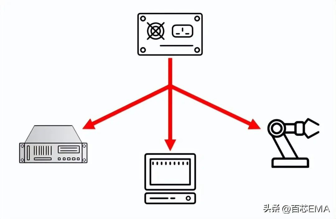
Star Grounding Diagram
2. Star Grounding in PCBs
Star grounding in PCBs mainly provides a single point where all ground return paths connect. This point is usually the negative power terminal (GND/DC common terminal on a typical power supply). For low-power AC systems, it may be the neutral line connection.
The star grounding in PCB layout is shown below (the blue part is the ground). It is suitable for audio PCBs, but improper grounding lacks measures to prevent external EMI.
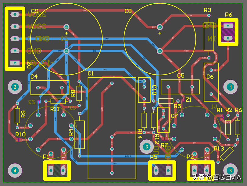
Star Grounding in PCB Layout (blue = GND)
3. Why is Star Grounding Often Not Recommended for PCBs?
Star grounding in PCBs must be used very carefully; improper use can cause the following problems:
① Ground Loops
If star grounding is used in digital signals, you cannot route traces between sections, as significant EMI will be generated.
In other words, any signal routed across the gap between two sections will encounter a very large power loop defining its return path.
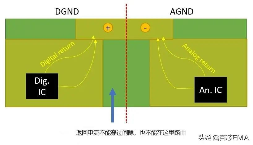
Signal crossing gap creates large ground loop
If the circuit operates at MHz or higher frequencies, and digital signals need to be routed to an interface near analog circuits, do not use star grounding. The return path will couple capacitively near the trace instead of spreading in the ground plane.
② EMI Issues Caused by Star Grounding
Placing all devices on the same PCB with overlapping GND planes at different potentials can prevent ground loops.
However, these planes are capacitively coupled. Capacitive coupling causes noise to be superimposed on signals read from one of the ground planes. Especially at higher frequencies, the continuous charging and discharging of the planes can produce EMI radiation.
Thus, solving ground loops introduces EMI radiation problems. In mixed-signal systems, the main EMI issues (both emission and susceptibility) come from routing restrictions imposed by star grounding.
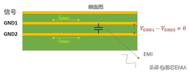
EMI Radiation
Star grounding with split planes creates EMI risks whenever a trace crosses a gap. In star grounding connected by traces, large gaps with strong radiation exist if the traces carry digital or high-frequency analog signals.
4. When to Use Star Grounding?
Star grounding is preferred in mixed-signal PCB design and power system design with split planes or trace-based star layouts:
- Circuits are completely isolated, sharing only one ground connection at the power supply, with no routing or bridging interfaces between sections (no A/D or D/A converters, etc.).
- Route these power rails separately and connect them only at the star point.
- Use a single ground point to minimize ground loop area and prevent analog/digital signal interference.
- Route different return paths as far apart as possible.
Creative routing is key to star grounding; you can even use ground pour areas on surface layers next to components.
Systems with multiple analog frequencies at multiple levels (shielding protects low-SNR analog lines more effectively than split planes).
Isolated power systems (including multi-rail systems) where plane splitting is used for galvanic isolation rather than noise control.
Note: Do NOT route signals across gaps between ground regions in a star grounding arrangement.
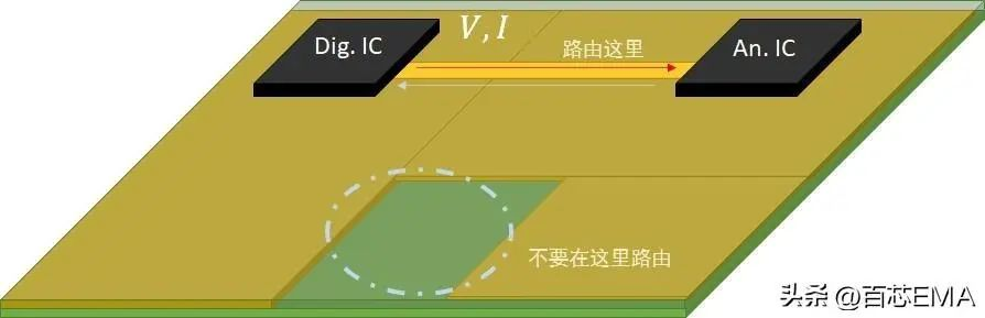
Do not route across ground gaps
5. Correct Method of Star Grounding in PCBs
The diagram below shows star grounding extended onto a PCB, with multiple separate ground regions that recombine at the power return. The shapes are complex, but the core idea is that all ground regions recombine at one point where the PCB connects back to the power supply.
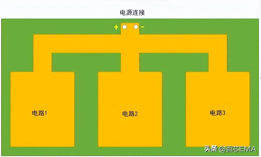
Wrong star grounding (recombining at power)
This method is incorrect. Below is the correct way to implement star grounding.
The correct method is to route signals only above their respective ground regions.
As mentioned above: never route signals across gaps between ground regions. Doing so creates a return path with a large loop area and generates EMI radiation.
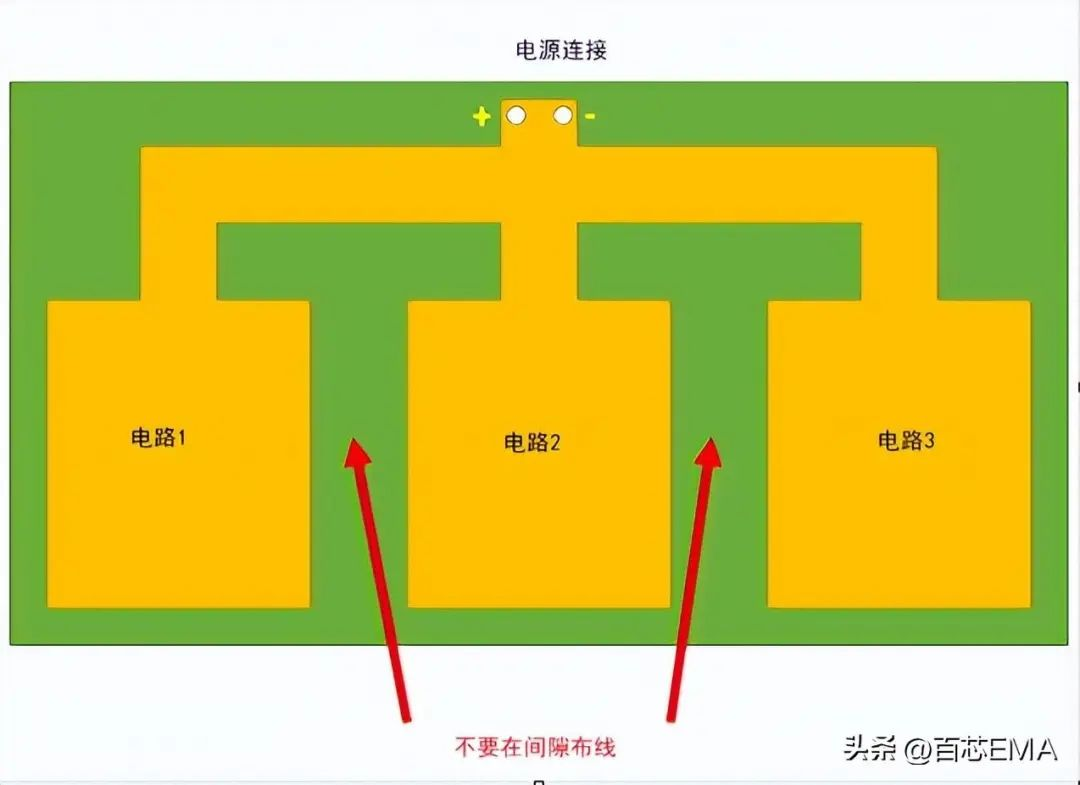
Correct star grounding (signal only above own ground)
This concludes the brief introduction to
star grounding in PCBs.
About Maxipcb
Maxipcb empowers innovators to turn cutting-edge technologies into reality.
We offer one-stop solutions for design, simulation, testing, PCB manufacturing, component procurement and SMT assembly, enabling efficient development, rapid deployment and risk control across the full product lifecycle.Serving the world in communications, industrial automation, aerospace, automotive, semiconductor and beyond, we build a safer, more connected future together.

 Star Grounding Diagram
 Star Grounding in PCB Layout (blue = GND)
 Signal crossing gap creates large ground loop
 EMI Radiation


 Wrong star grounding (recombining at power)
 Correct star grounding (signal only above own ground)