FPC (Flexible Printed Circuit) is now widely used in modern electronic products and is familiar to most engineers. Characterized by its thinness, light weight, and bendability, FPC can be processed into arbitrary shapes and sizes, complementing rigid FR-4 PCBs. However, FPC differs from rigid PCBs in design, with specific considerations to note.
FPC (Flexible Printed Circuit) is now widely used in modern electronic products and is familiar to most engineers. Characterized by its thinness, light weight, and bendability, FPC can be processed into arbitrary shapes and sizes, complementing rigid FR-4 PCBs. However, FPC differs from rigid PCBs in design, with specific considerations to note. This guide details 8 core FPC design key points to help avoid common pitfalls:
- Outline and Drilling Design
- Trace Design
- Edge Gold Finger Design
- Solder Mask Design
- Silkscreen Design
- Panelization Design
- Stiffener Design
- Board Thickness Specification
FPC design for drilling, board outline, traces, solder mask, and silkscreen shares similarities with PCB, but stiffener layers are required on the back of components and at connector positions. Below are the critical design details and pitfalls for each aspect:
1. Outline and Drilling Design
(1) The minimum distance between a through-hole and the board outline must be
0.5 mm; if less than 0.5 mm, the hole must be modified to a U-shaped hole (connected to the board outline).
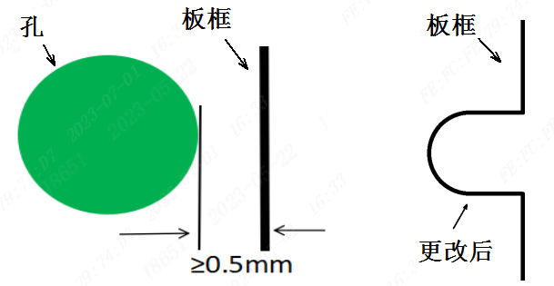
Through-hole to board outline: original (too close) vs modified U-shaped hole
(2) Maintain a distance of
≥0.2 mm between vias and solder mask openings; otherwise, copper exposure at the hole edge will occur.
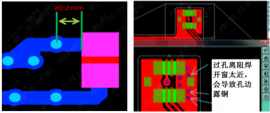
Via too close to solder mask opening causing copper exposure at the edge
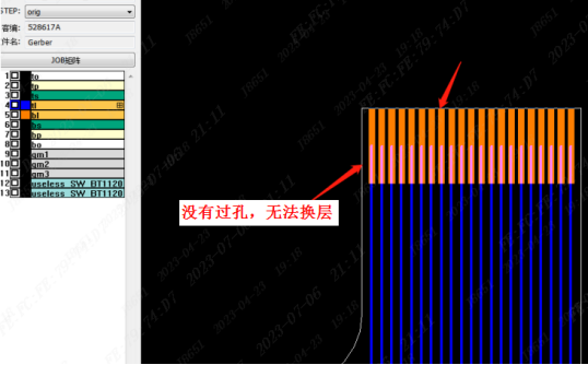
(3)
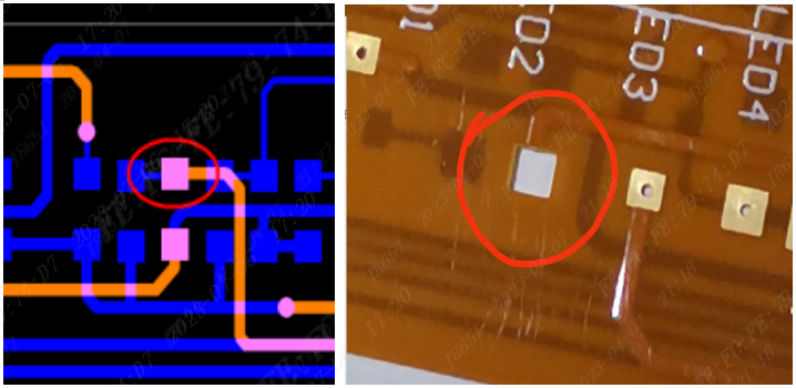
Via-in-pad is not recommended for FPC. Resin plugging is not feasible for FPC, and via-in-pad may lead to solder leakage during soldering.
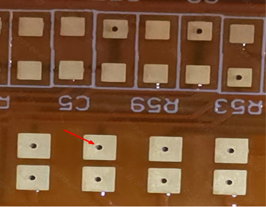
FPC via-in-pad design with solder leakage risk
2. Trace Design
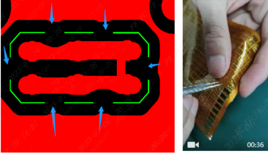
(1)
Large copper area oxidation: Air is difficult to expel during lamination of large copper areas; moisture in the air reacts with copper at high temperature and pressure, causing oxidation and poor appearance (functional performance is unaffected). Solution: Use
grid copper or add solder mask openings on large copper areas.
Oxidized large copper area vs optimized grid copper design
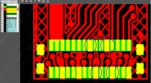
(2)
Avoid isolated pads as much as possible: Isolated pads (especially overlapping on both sides) are prone to peeling due to the thin FPC base material (only 25 μm). Solution: Add copper pouring, connect the pad to the pour with 4-corner traces, and
stagger pads on the top and bottom layers to enhance adhesion.
Isolated pad design (prone to peeling) vs optimized pad with copper pouring and staggered layers
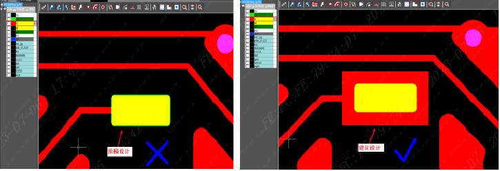
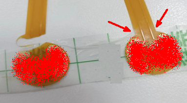
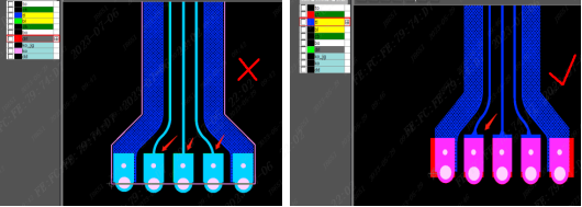
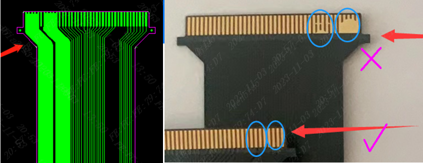
(3)
Connector pad peeling: Independent connector pads are highly susceptible to peeling;
solder mask over pad (SMOP) design is recommended.
Original connector pad vs SMOP optimized pad
(4)
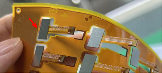
Avoid large exposed copper areas as they may cause wrinkling of the FPC.
Large exposed copper area with obvious wrinkling
(5) FPC uses coverlay as the solder mask layer (coverlay is cut and then laminated). Require
0.2 mm spacing between pads and traces; a
solder mask bridge of ≥0.5 mm is needed (i.e., pad-to-pad spacing ≥0.5 mm to retain the bridge). If the spacing is insufficient, full opening is required (with exposed traces accepted).
FPC coverlay opening with standard pad-trace spacing and solder mask bridge
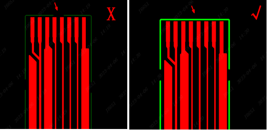
(6)
Tear resistance for sparse flat cables: Sparse traces at corners are prone to tearing. Solution: Add
anti-tear copper strips at the board edge or ground copper on the back layer.
Sparse flat cable with corner tearing risk vs optimized design with anti-tear copper strips
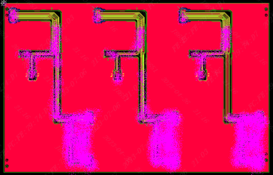
(7) Use
45° grid copper for better signal transmission; the recommended trace width/space is
0.2/0.2 mm.
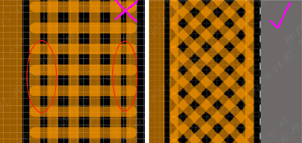
45° grid copper for FPC vs random grid copper
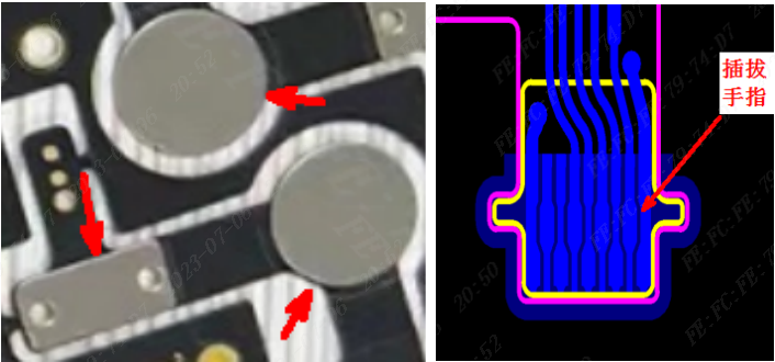
3. Edge Gold Finger Design
(1)
Plug-in gold fingers: High-temperature carbonization during laser cutting may cause micro-shorts between gold fingers. Gold fingers must be
recessed 0.2 mm from the board edge (standard for JLCPCB; special requirements need to be noted).
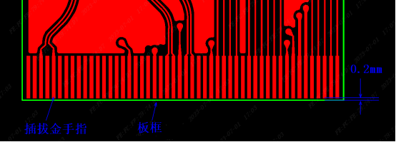
Plug-in gold finger recessed 0.2 mm from the board edge
(2)
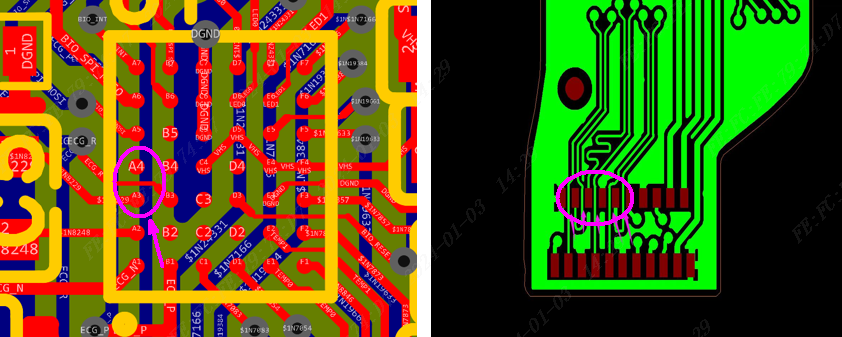
Soldered gold fingers: Vias on inner pads cannot be arranged in a straight line to prevent stress concentration and trace fracture.
Original via alignment (prone to fracture) vs optimized staggered via design for soldered gold fingers
(3) Coverlay on the top and bottom of soldered gold fingers must be
staggered ≥0.3 mm to prevent bending fracture.
Staggered coverlay design for soldered gold fingers
(4) Soldered gold fingers are recommended to use
SMOP design (extend the pad so the coverlay overlaps the pad by ≥0.3 mm).
SMOP design for soldered gold fingers with coverlay overlapping the pad
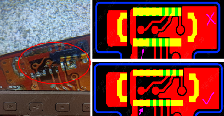
(5)
Solder mask opening for gold fingers: The opening should overlap the pad by ≥0.3 mm to prevent separation between the gold finger pad and its connection.
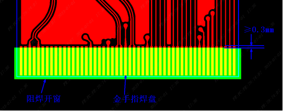
Gold finger solder mask opening with 0.3 mm pad overlap
(6) Hollowed boards are not supported; reverse gold fingers require additional pads and vias to achieve layer transition.
Reverse gold finger design with layer transition via pads and vias
(7) FPC coverlay cannot form solder mask bridges like green oil on PCBs. For IC pad design,
no extra copper pouring on pads is allowed (excess copper causes larger pad size, smaller spacing, and soldering short circuits).
Unreasonable IC pad design with extra copper (prone to short) vs optimized clean pad design
(8) Gold finger pads must be
independent; copper pouring or traces on gold finger pads will cause exposed copper/traces after solder mask opening.
Gold finger pad with copper pouring (exposed copper) vs independent gold finger pad
(9) The default tolerance for gold finger outline is
±0.1 mm; for a tighter tolerance of
±0.05 mm, select the personalized service option when placing an order.
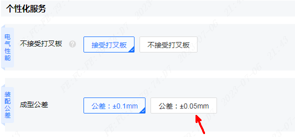
MaxiPCB order interface for gold finger outline tolerance selection
4. Solder Mask Design
(1) FPC connector pads are prone to peeling;
SMOP design is recommended.
Original connector pad vs SMOP design with retained solder mask bridge
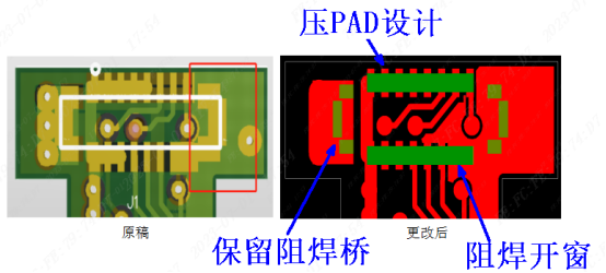
(2) A connecting bridge is required in the middle of IC pads to retain the central solder mask bridge.
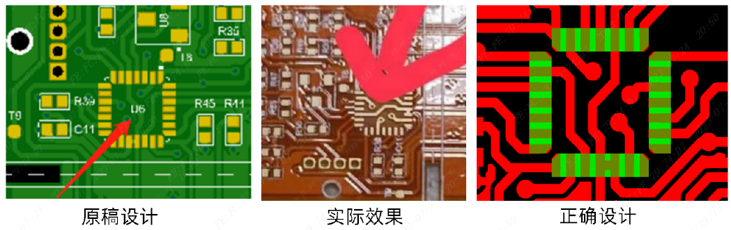
IC pad with central connecting bridge for solder mask bridge retention
(3)
Solder mask opening is mandatory for gold finger pads; otherwise, conduction with the connector will fail.
Gold finger pad with proper solder mask opening (for conduction) vs no opening (no conduction)
(4) Coverlay is the default solder mask layer; ensure the solder mask layer is correctly defined in the design (avoid missing openings).
FPC with missing solder mask opening (defect) vs correct solder mask opening
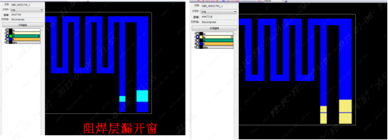
(5) To prevent copper fracture at vias during bending, FPC vias are
covered with solder mask by default; note opening requirements in the order if vias need to be exposed.
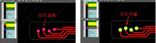
FPC via with solder mask cover (default) vs exposed via (custom)
(6) Test points with via attributes may fail to be processed;
do not set test points as vias, or add independent openings for test points.
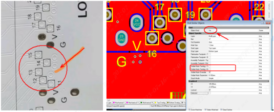
Unprocessable test point with via attribute vs optimized test point with independent opening
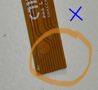
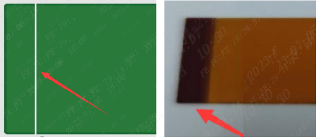
(7) Large exposed gold areas on the edge of double-sided FPC may cause edge blackening; add a circle of coverlay at the board edge to solve this.
FPC edge with blackening (exposed gold) vs optimized edge with coverlay
5. Silkscreen Design
(1) If silkscreen is required on stiffeners, select the
"silkscreen on stiffener" option when placing an order to prevent production process errors.
MaxiPCB order interface for silkscreen on stiffener selection
(2)
Do not place explanatory text inside the FPC active area to avoid damage or interference with circuit functionality.
FPC with silkscreen in active area (defect) vs silkscreen on non-active area
6. Panelization Design
(1) FPC with full steel sheet stiffeners is heavy and prone to tensile deformation (making SMT impossible). Requirements:
≥3 mm spacing between boards; 0.5 mm slot width; 1 mm connecting tab width (add a tab every ~15 mm). Note in the order: "pack with paper between each piece and cardboard on top/bottom for shipping".
Panelization for steel sheet stiffened FPC with standard spacing and connecting tabs
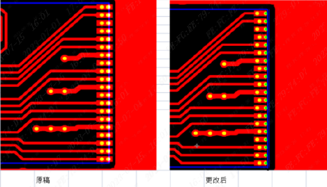
(2)
Do not place connecting tabs on gold fingers as this will cause uneven gold finger tips.
Incorrect panelization with connecting tab on gold finger vs correct tab position on non-gold finger area
(3) Insufficient connecting tabs cause board separation during production;
at least 2 tabs per piece (0.8 mm width) are required (more tabs for larger boards).
FPC panel with insufficient tabs (board separation) vs optimized panel with enough tabs
(4) Excessive connecting tabs on small boards make manual depaneling difficult; for non-SMT small boards,
2 tabs of 0.3 mm width are sufficient for easy hand tearing.
Small FPC board with excessive tabs (hard to depanel) vs 2 small tabs (easy hand tearing)
(5) Low panel utilization leads to higher pricing; design panels with a width of
119 mm or 240/250 mm for optimal utilization (third-party panelization is recommended for special sizes).
FPC panel with low utilization vs high-utilization standard width panel
(6) Small FPC boards (<20×20 mm) may be sucked away during laser dust collection;
panelize for delivery or request JLCPCB to depanel after production.
Tiny FPC board (20×20 mm) with suction risk vs panelized tiny boards
7. Stiffener Design
Stiffeners are rigid materials added to local FPC areas for easy assembly:
- PI stiffeners: For gold finger plug-in products
- FR4 stiffeners: For low-end products
- Steel sheet stiffeners: High flatness, no deformation – for chip SMT products
(1)
Do not use steel sheet stiffeners for through-hole pins (risk of short circuit); steel sheets have weak magnetism (not for Hall effect components); steel sheet stiffeners are not recommended for plug-in gold fingers.
Steel sheet stiffener on through-hole pins (short circuit risk) vs PI stiffener replacement
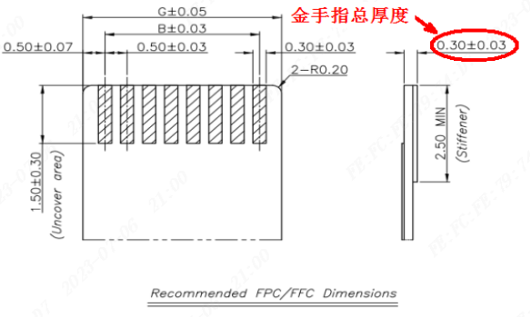
(2) For FPC with plug-in gold fingers, note the
total thickness requirement in the order (specified in the connector datasheet). Do not calculate PI stiffener thickness by simply subtracting FPC thickness from total thickness; use the JLCPCB gold finger PI thickness calculator for accurate values.
MaxiPCB gold finger PI thickness calculator interface
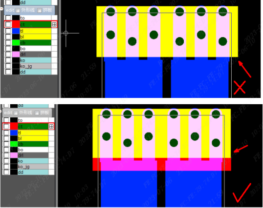
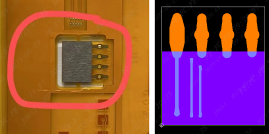
(3)
Stiffener cutout design: Stiffeners must avoid component holes/pads below (customer-designed cutouts are preferred). JLCPCB defaults to a
0.3 mm clearance from pads; if the remaining stiffener width after cutout is <2 mm, the stiffener will be fully removed (no notice for this; special requirements need to be noted).
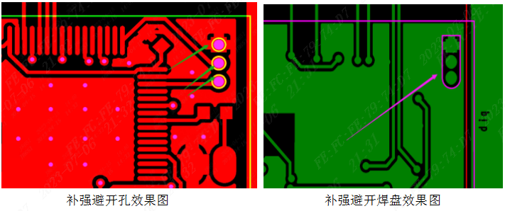
Stiffener cutout for component holes/pads with 0.3 mm clearance
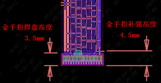
(4) The height of the gold finger stiffener is recommended to be
≥1.0 mm longer than the gold finger pad to prevent gold finger fracture during use.
Gold finger stiffener longer than the pad (anti-fracture) vs stiffener flush with the pad (fracture risk)
(5) EMI shielding film may conduct on both sides;
cancel the EMI film if the underlying traces are different nets.
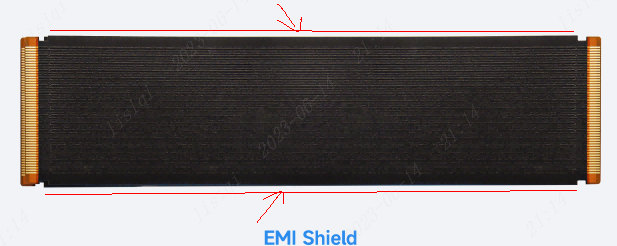
EMI shielding film on mixed nets (conduction risk) vs EMI film removed
(6) For specific EMI film ground resistance requirements, design the ground solder mask opening by yourself; JLCPCB adds a
≥1.0 mm random opening by default if no requirements are specified.
Note: Ungrounded EMI film may absorb a large amount of electromagnetic waves and cause signal issues –
prototype verification is mandatory.
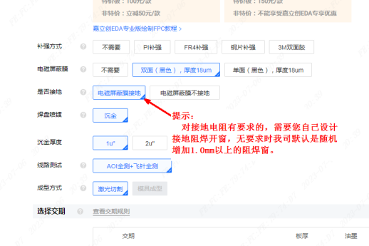
MaxiPCB order interface for EMI shielding film grounding selection
(7)
Do not attach steel sheets to pads as this will cause short circuits.
Steel sheet attached to pad (short circuit) vs steel sheet with cutout for pads
(8)
FR4 stiffener width: Narrow FR4 stiffeners are prone to fracture and carbonization; replace FR4 stiffeners with width <5 mm with PI or steel sheet stiffeners. The minimum width of adhesive backing must be
≥3 mm.
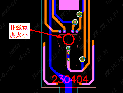
Narrow FR4 stiffener (fracture risk) vs optimized PI stiffener
(9)
No stiffeners/adhesive backing around SMT pads – this will prevent solder paste printing. If stiffeners are necessary, perform
SMT first, then attach stiffeners/adhesive backing.
SMT pad with stiffener (no solder paste printing) vs stiffener attached after SMT
8. Board Thickness Specification
FPC total thickness includes coverlay, copper thickness, and PI base material thickness; the thickness will be reduced for areas without copper or coverlay – pay close attention during design.
Standard FPC Stackup and Thickness (Excluding Stiffener and Silkscreen Ink)
-
2-layer FPC
- 0.11 mm: PI(12.5μm) + Adhesive(15μm) + Cu(12μm) + PI(25μm) + Cu(12μm) + Adhesive(15μm) + PI(12.5μm) (Total: 104μm)
- 0.12 mm: PI(12.5μm) + Adhesive(15μm) + Cu(18μm) + PI(25μm) + Cu(18μm) + Adhesive(15μm) + PI(12.5μm) (Total: 116μm)
- 0.20 mm: PI(25μm) + Adhesive(25μm) + Cu(35μm) + PI(25μm) + Cu(35μm) + Adhesive(25μm) + PI(25μm) (Total: 195μm)
-
1-layer FPC
- 0.07 mm: PI(12.5μm) + Adhesive(15μm) + Cu(18μm) + PI(25μm) (Total: 70.5μm)
- 0.11 mm: PI(25μm) + Adhesive(25μm) + Cu(35μm) + PI(25μm) (Total: 110μm)
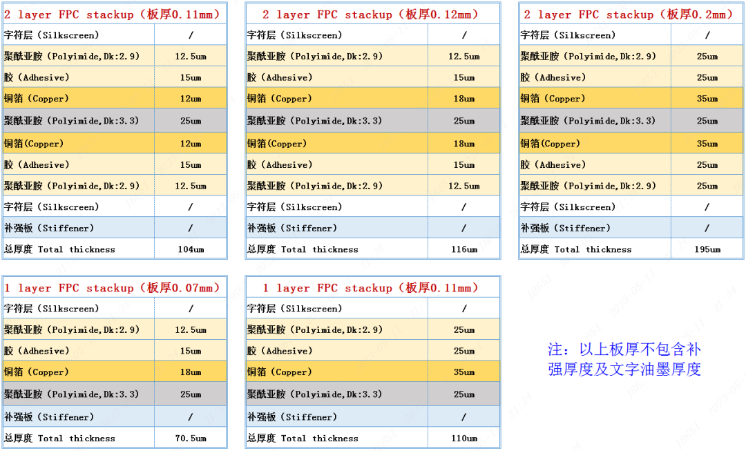
Standard 1-layer/2-layer FPC stackup with detailed thickness parameters
About Maxipcb
Maxipcb empowers innovators to turn cutting-edge technologies into reality.
We offer one-stop solutions for design, simulation, testing, PCB manufacturing, component procurement and SMT assembly, enabling efficient development, rapid deployment and risk control across the full product lifecycle.Serving the world in communications, industrial automation, aerospace, automotive, semiconductor and beyond, we build a safer, more connected future together.


