In PCB (Printed Circuit Board) design, via parasitic inductance is an important consideration. When current passes through a PCB via, a certain amount of parasitic inductance is generated due to the via’s geometric shape and layout. This parasitic inductance may affect circuit performance, so it needs to be calculated and taken into account.
In PCB (Printed Circuit Board) design, via parasitic inductance is an important consideration. When current passes through a PCB via, a certain amount of parasitic inductance is generated due to the via’s geometric shape and layout. This parasitic inductance may affect circuit performance, so it needs to be calculated and taken into account.
Inductance refers to a conductor’s or coil’s ability to respond to changes in current. When current flows through a conductor or coil, a magnetic field is generated. This magnetic field in turn induces an electromotive force inside the conductor or coil, thereby opposing changes in current. This phenomenon is called self-inductance, which is one of the basic characteristics of inductance.
① Unit: The unit of inductance is Henry (H).
② Applications: Inductors are widely used in electronic circuits, communication systems, energy transmission, and other fields—for example, in filtering, impedance matching, and energy storage.
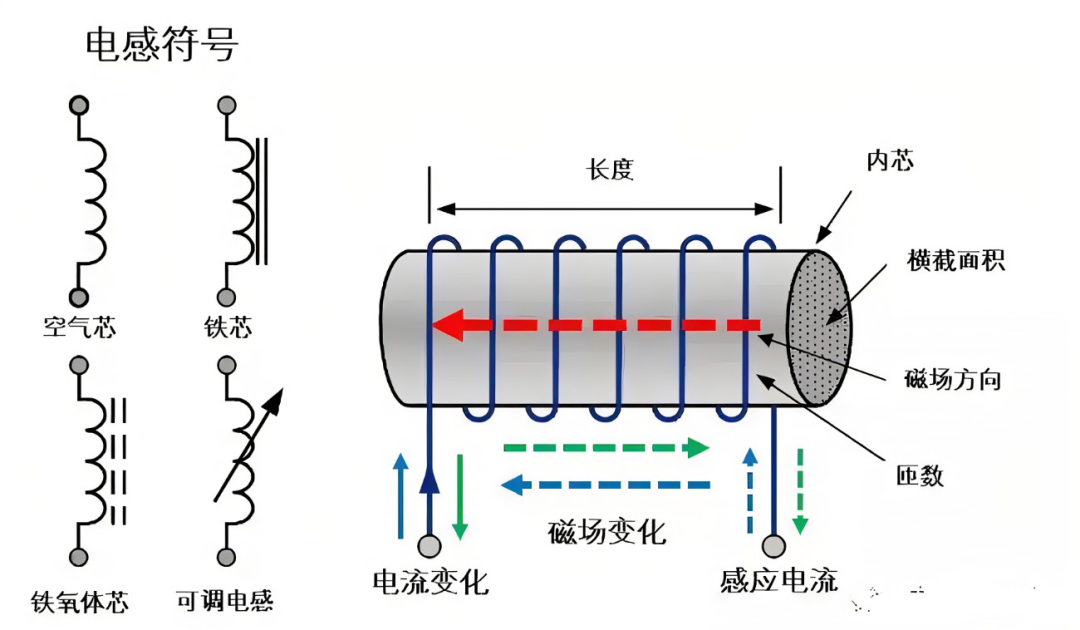
Inductor-related diagram, including inductor symbols, structural diagrams of air-core, iron-core, variable, and ferrite-core inductors, as well as labels for key parameters such as length, inner core, cross-sectional area, magnetic field direction, number of turns, magnetic field change, current change, and induced current
Methods for Calculating Via Parasitic Inductance
There are various methods to calculate via parasitic inductance, and one common approach is estimation using an inductance formula. For cylindrical vias, the following formula can be used to calculate their parasitic inductance:
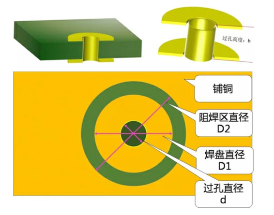
Via structure parameter diagram, labeling via height (h), copper pour, solder mask area diameter (D2), pad diameter (D1), and via diameter (d)
Where:
- (L) = Parasitic inductance (unit: Henry, H)
- (μ) = Permeability of air, usually taken as 4π×10−7 H/m (or the permeability of the specific medium)
- (N) = Number of turns of the via
- (A) = Effective cross-sectional area of the via (unit: square meters, m²)
- (l) = Length of the via (unit: meters, m)
① Calculation Steps
- Determine the via’s geometric parameters: Include parameters such as the via’s diameter and length.
- Calculate the via’s effective cross-sectional area: For a cylindrical via, the cross-sectional area is the area of a circle, i.e., A=π⋅r2 (where r is the via’s radius).
- Determine the number of via turns: The number of turns depends on the wiring around the via and interlayer connection methods.
- Select the appropriate permeability: Calculate parasitic inductance based on the actual material’s permeability.
- Substitute parameters into the formula: Plug the above parameters into the formula to obtain the via’s parasitic inductance value.
② Notes
When calculating via parasitic inductance, the following points need to be considered:
- Geometric shape: The via’s geometric shape affects the calculation result; cylindrical vias are the most common type.
- Material properties: Different materials have different permeabilities, so the actual material’s permeability must be used for calculation.
- Number of turns and length: The via’s number of turns and length directly affect the parasitic inductance value—these parameters need to be measured accurately.
- Influencing factors: Parasitic inductance affects the bandwidth and speed of signal transmission, so special attention is required when designing high-frequency circuits.
By calculating via parasitic inductance, potential impacts in the circuit can be better understood, and corresponding measures can be taken during the design phase to reduce unnecessary interference. In PCB design, reasonably considering parameters such as parasitic inductance helps improve circuit performance and stability, ensuring the circuit operates normally.
To reduce the impact of via parasitic inductance, the following measures can be taken during PCB design:
① Reasonable via layout: Avoid overcrowding of vias and minimize mutual interference between vias.
② Reduce via length: Shorten the via’s length as much as possible to lower the parasitic inductance value.
③ Increase via diameter: Increasing the via’s diameter can reduce parasitic inductance and improve signal transmission performance.
About Maxipcb
Maxipcb empowers innovators to turn cutting-edge technologies into reality.
We offer one-stop solutions for design, simulation, testing, PCB manufacturing, component procurement and SMT assembly, enabling efficient development, rapid deployment and risk control across the full product lifecycle.Serving the world in communications, industrial automation, aerospace, automotive, semiconductor and beyond, we build a safer, more connected future together.


