I. What is Inrush Current
Inrush current refers to the peak or overload current that is much larger than the steady-state current generated at the moment the power supply is turned on or when an abnormality occurs in the circuit; inrush is also called a surge. Essentially, a surge is a violent pulse that occurs in just one microsecond.
The nonlinearity of the circuit itself may produce pulses higher than those of the power supply; or the power supply or other parts of the circuit may be disturbed by internal or external sharp pulses, as well as external factors such as lightning and ESD. This is likely to burn out the circuit in an instant of the surge, such as breakdown of PN junction capacitance, burnout of resistors, and so on.
Inrush current protection is a protection circuit designed by utilizing the sensitivity of nonlinear components to high frequencies (surges). A simple and commonly used method is to connect large and small capacitors in parallel and inductors in series. The sources of surges in power supply systems are divided into external (caused by lightning) and internal (start-stop and faults of electrical equipment, etc.). From the perspective of electronic engineering, the sources of system surges are defined into three categories: lightning, static electricity, and switching circuits.
II. Inrush Suppression Schemes
There are two common schemes for inrush design: one is to use a fusible resistor (fuse resistor), and the other is to use a voltage clamping device (surge discharge tube, varistor, etc.). According to the test method of surge (shock) immunity specified in GB/T17626.5, 10 surges are applied at each of the four phases of 0°, 90°, 180°, and 270° of the mains supply.
III. Discharge Teeth
Discharge teeth, also known as discharge gaps or spark gaps, are a pair of acute-angled triangles pointing to each other, fabricated using copper foil layers during PCB routing. These triangles must be placed on another layer of the PCB board away from the components and cannot be covered by green solder mask or other materials.
During surge testing or ESD testing, a high voltage will be generated across the common mode inductor, resulting in arcing. If the distance to surrounding components is too close, it may damage the surrounding components. Therefore, a discharge tube can be connected in parallel across it to suppress the voltage. As shown in the figure below, FU2 is a gas discharge tube connected in parallel across the common mode inductor, which can achieve an arc-extinguishing effect.
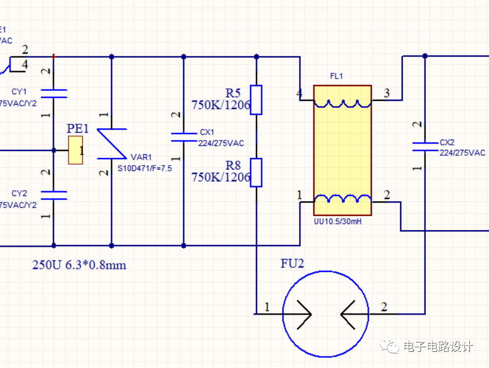
(AC, FL1, CY1, R5, PE1, CX1, CX2, VAR1, R8, CY2, UU1, FU2 with parameters: 75VAC/Y2, 750K/1206, 224/275VAC, S10D471/F=7.5, 0.5/30mH, 250U 6.3*0.8mm)
Gas discharge tubes have an excellent suppression effect but relatively high cost. In many cases, we place discharge teeth across the common mode inductor during PCB design, allowing the common mode inductor to discharge through the tips of the discharge teeth. This can reduce or even avoid discharge through other paths and protect the surrounding and subsequent-stage components.
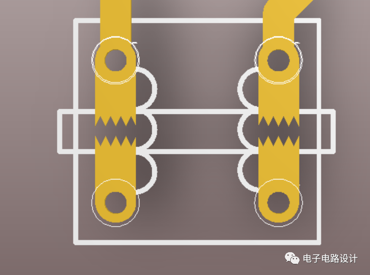
Schematic of PCB-designed discharge teeth for surge suppression
This type of discharge tooth discharges in the form of air breakdown, so attention should be paid to placing it on a different layer from the common mode inductor during design. Although it can achieve a certain effect, in occasions where inrush current/voltage and ESD occur frequently, the use of such discharge teeth is prone to carbon deposition, which will cause a short circuit over time and go against the original design intention.
About Maxipcb
Maxipcb empowers innovators to turn cutting-edge technologies into reality.
We offer one-stop solutions for design, simulation, testing, PCB manufacturing, component procurement and SMT assembly, enabling efficient development, rapid deployment and risk control across the full product lifecycle.Serving the world in communications, industrial automation, aerospace, automotive, semiconductor and beyond, we build a safer, more connected future together.


 (AC, FL1, CY1, R5, PE1, CX1, CX2, VAR1, R8, CY2, UU1, FU2 with parameters: 75VAC/Y2, 750K/1206, 224/275VAC, S10D471/F=7.5, 0.5/30mH, 250U 6.3*0.8mm)