Our designed DC-DC power supplies generally include components such as capacitors, inductors, Schottky diodes, resistors, and integrated circuits. The conversion efficiency of power products cannot reach 100%, so power loss is inevitable. These losses are manifested as temperature rise, and poor thermal design will accelerate the lifespan degradation of the power system.
Our designed DC-DC power supplies generally include components such as capacitors, inductors, Schottky diodes, resistors, and integrated circuits. The conversion efficiency of power products cannot reach 100%, so power loss is inevitable. These losses are manifested as temperature rise, and poor thermal design will accelerate the lifespan degradation of the power system. Therefore, thermal design is particularly critical in system reliability design. However, thermal design is also very challenging, as it involves many factors such as PCB dimensions and air flow conditions.
When reading IC datasheets, we often encounter terms such as RθJA, TJ, TSTG, and TLEAD.
- RθJA: Thermal resistance of the chip, defined as the junction temperature rise per 1W of power dissipation.
- TJ: Junction temperature of the chip.
- TSTG: Storage temperature range of the chip.
- TLEAD: Processing temperature of the chip leads.
Term Explanation
First, understand the temperature-related terms:
TJ,
TA,
TC,
TT.
As shown in
Figure 1:
- TJ: Junction temperature inside the chip.
- TA: Ambient temperature around the chip.
- TC: Temperature of the back pad or bottom case of the chip.
- TT: Surface temperature of the chip.
The common thermal performance parameter in datasheets is
RθJA (junction-to-ambient thermal resistance).
The core formula:
TJ = TA + (RθJA × PD)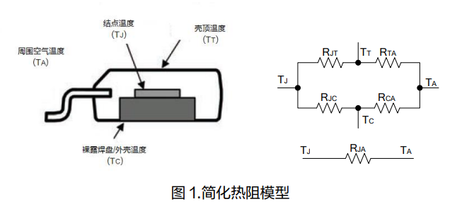
Simplified thermal resistance model
(Junction temperature (TJ), Top case temperature (TT), Ambient temperature (TA), Exposed pad/case temperature (TC); thermal resistances RθJT, RθJC, RθCA, RθJA)
Heat generated by the chip mainly dissipates through two paths:
- From chip junction to top molding compound (RθJT), then to ambient air via convection/radiation (RθTA).
- From chip junction to back pad (RθJC), then to PCB surface and ambient air via convection/radiation (RθCA).
For chips without an exposed thermal pad, RθJC refers to the junction-to-top-molding thermal resistance, as it represents the lowest thermal resistance path from the internal junction to the outside.
Typical Thermal Resistance Values
Table 1 Typical Thermal Resistance
It can be seen that thermal resistance is related to PCB size, air flow, PCB thickness, via count, and other parameters.
Design Example
Buck converter:
- Output: 5V, 1A
- Efficiency η = 90%
- Ambient temperature TA = 50°C
- Capacitor rated temp = 100°C (close to the chip)
- Target junction temperature TJ ≤ 90°C
Step 1: Calculate power dissipation PD
PD = VOUT × IOUT × (1/η − 1) = 5×1×(1/0.9−1) ≈ 0.56W
Step 2: Required thermal resistance
RθJA ≤ (TJ − TA) / PD ≤ (90−50)/0.56 ≤ 71.4°C/W
Step 3: Thermal design methods
-
PCB Size
Select a chip with RθJA < 71.4°C/W (e.g., SOP8-EP, RθJA=60°C/W).
Under natural convection (no fan, no heatsink), double-sided copper-clad PCB area requirement:
PCB Area (cm²) ≥ 15.29 × PD = 15.29×0.56 ≈ 8.56 cm²
-
Thermal Vias
Thermal resistance of vias:
RVIAS = 261°C/W ÷ Number of vias
Increasing via count effectively reduces thermal resistance.
-
Copper Thickness
Thermal resistance of copper:
RCu = (1/λCu × Length) ÷ (Width × Thickness)
λCu = 4W/(cm·°C)
Thicker copper reduces thermal resistance.
-
Heatsink
Heatsinks effectively lower chip temperature.
- Mounted on top of molding compound (high RθJT, poor contact).
- Connected to backside thermal vias (better performance).
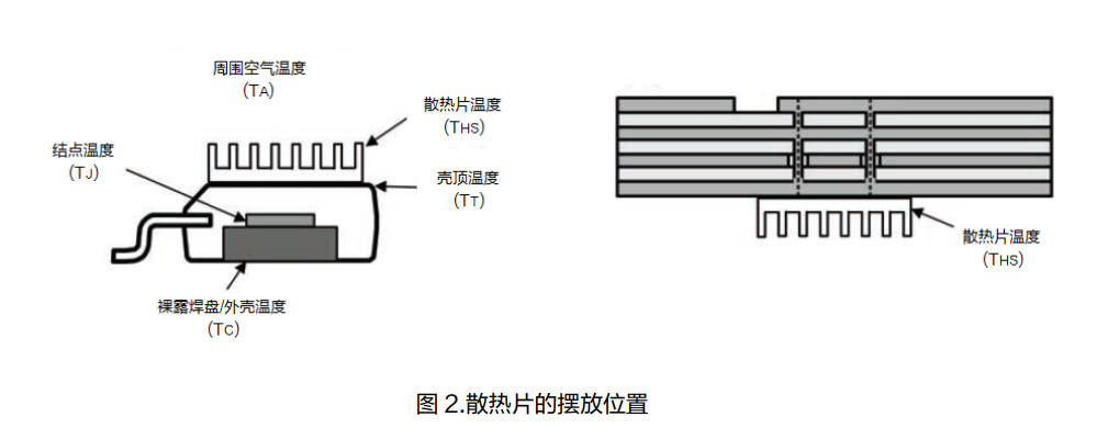
Heatsink placement
(Ambient temp TA, Heatsink temp THS, Junction temp TJ, Top case temp TT, Exposed pad temp TC)
-
Air Cooling
In large, non-sealed spaces, low-power fans significantly reduce overall thermal resistance.
-
Potting
For waterproof, dustproof, and shockproof products, thermal silicone gel transfers heat from components to the outer casing.
About Maxipcb
Maxipcb empowers innovators to turn cutting-edge technologies into reality.
We offer one-stop solutions for design, simulation, testing, PCB manufacturing, component procurement and SMT assembly, enabling efficient development, rapid deployment and risk control across the full product lifecycle.Serving the world in communications, industrial automation, aerospace, automotive, semiconductor and beyond, we build a safer, more connected future together.


