You already know that all electronic equipment consists of circuit boards. PCB or printed circuit board is an integral part of today's electronic products. A green board with complex lines and patterns is called PCB. In electronic equipment, the marks on the PCB can ensure that all components work together smoothly. The manufacture of PCB consists of many components and steps.
You already know that all electronic equipment consists of circuit boards. PCB or printed circuit board is an integral part of today's electronic products. A green board with complex lines and patterns is called PCB. In electronic equipment, the marks on the PCB can ensure that all components work together smoothly. The manufacture of PCB consists of many components and steps. The final stage of manufacturing printed circuit board (PCB) is to add screen printing on the top layer.
Screen printing is the process of painting ink marks on the circuit board to identify its components, warning symbols, test points, marks, logo marks, etc. Usually, the component part is the screen printed side of the manufacturer. It occasionally appears in the welding channel, but the cost of getting there is high. Screen printing of PCB helps manufacturers and designers to quickly identify the layout of components. Screen printing of PCB will ensure that parts can be reassembled. Screen printing will provide engineers or technicians with instructions on where and how components should be placed on PCB.
This article will provide all the information you need to know about PCB screen printing, including why it is so important, what is the best practice and how to correctly incorporate it into PCB design.
What is PCB screen printing?Imagine that you are doing a DIY project to build a futuristic smart watch from scratch. Your PCB is like the blueprint of this high-tech wearable device. Screen printing is a way for you to add visual marks and labels to guide you and anyone involved in the assembly process.
Screen printing on PCB is a layer of ink printed on the surface of circuit board. It is usually made of polymer or ceramic materials and is applied by screen printing. The ink is applied through a mesh screen, which acts as a template for the desired pattern. The screen is placed on the PCB, and the ink is forced to pass through the screen and reach the circuit board. The standard screen colors used by manufacturers are black, yellow and white. When using PCB software, common fonts can be used in the design of screen printing layer.
It is usually applied to the top and bottom layers of circuit boards. Using screen printing, the surface of PCB can be printed with text, labels and symbols. Components, their locations, part names, component numbers, brand logos and other information are all presented visually.
Although the silk screen layer has nothing to do with the actual electrical operation of the circuit board, it is very important for the construction, testing and use of the circuit board. Help find things and put them in the right place so that everything is in order and in the right direction. It is very useful for the assembly process because it provides easy-to-understand visual clues for technicians and assemblers. Now that you know the basics of screen printing of printed circuit boards, let's look at its wider uses.
What information does PCB screen printing have?As mentioned above, screen printing on PCB may have no effect on the function of PCB; However, its value lies in the information it provides. For example, it will help anyone:
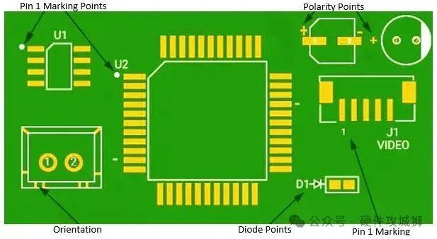
Warning symbol: identifies the warning symbol that highlights the high-temperature components that need the user's attention and care during operation.
Polarity: Know the polarity of components to install components correctly. Pin marks provide orientation information to ensure accurate assembly.
Test point: locate the test point indicator on the silk screen to assist the design engineer in PCB testing and debugging.
Reference indicator: a unique identifier for each assembly position on PCB to identify components by reference indicator.
Numbers: Unique numbers are found on PCB screen printing, indicating manufacturer's mark, version number, etc.
Component symbols: For special components such as diodes and optocouplers, the component symbols printed on screen printing can ensure accurate alignment during installation.
Switch setting: the default switch setting is the instructions on PCB screen printing, which enhances the usability of the circuit board.
Dense components: The PIN on screen printing is helpful for testing and debugging compact components such as ball grid array (BGA).
Troubleshooting and repair: Screen printing marks can easily identify and locate various components, thus speeding up the repair process.
Manufacturing documents: Screen printing marks provide necessary manufacturing and assembly documents. This includes copyright notice, company logo, production date and other important quality control and traceability details.
Brand: these marks contribute to the beauty and brand of PCB. Combining brand elements, logos and selected colors can enhance the overall visual appeal and professionalism.
What is the best thickness of screen printing on PCB?The thickness of screen on PCB is affected by the screen size and the amount of ink used. Generally speaking, screen printing in PCB is realized as a fine coating, and the thickness is usually below 0.1 mm. In this way, the ink can be accurately applied without significantly changing the overall thickness of the PCB.
The depth of screen on PCB may vary due to various factors, including manufacturing methods, specific requirements and established standards in the industry. Generally, compared with other layers in PCB, the depth of screen printing on PCB is relatively thin.
In some cases, the thickness of screen printed PCB layer is usually about 0.02 mm to 0.1 mm (20 to 100 microns). It is very important to consider that these measurements are rough approximations and may vary according to various factors.
Although the screen in the printed circuit board is relatively thin, it still provides sufficient visibility and elasticity for the mark. The thickness is carefully monitored to ensure that it will not damage the function of PCB, trigger misalignment of components or cause complications in the manufacturing process.
PCB screen printing design guideThe first step is to use professional software such as AutoCAD or EAGLE to develop screen printing layer. This design contains all relevant texts, symbols and marks for locating and assembling PCB components. You need software skills to develop screen printing layouts. You should also be familiar with the standard layout requirements to achieve positive results.
Color selection
The color of screen printing should be carefully considered. Dark colors such as black and dark blue are not always the best choice because they are bad for the eyes. Try using contrasting colors to make them visible on the PCB.
information
When designing screen printing, only the most relevant details about the circuit and its components should be included. If something has been covered elsewhere on the PCB, there is no need to repeat it here.
Text size
In order to ensure correct data interpretation, the screen-printed fonts on the printed circuit board (PCB) must be readable.
The text size and line width will change according to the screen printing technology. The recommended minimum font size for conventional screen printing is 50 mil and the minimum line width is 7 mil. Remember, just because you can reduce the text size doesn't mean you should. When font size and line spacing decrease, printing and understanding text becomes more challenging.
Only two directions should be used to make screen printing easier to read. Reference indicators should be read from left to right and from bottom to top to obtain uniform and clear screen printing.
Don't overlap
Numbers, component names and other detailed information printed on the PCB wire should not overlap as much as possible. However, in order to avoid part of the screen printing being removed during the formation of the solder mask window, the screen printing must not overlap with the through hole or pad. There should be at least 5 million gaps between screen printing elements.
accurate positioning
It is best to place reference indicators near the components they identify. It is best to keep the reference designator in one rotation, although this is only sometimes feasible, especially when dealing with tiny discrete parts.
To prevent users from constantly rotating the panel to see the next indicator, try to limit the rotation to 0 to 90 degrees.
PCB screen printing label marking
Avoid screen printing on vias and holes, and ensure that no components obscure reference indicators or other important circuit board information. If you need to help yourself decipher the software design, consider how the end user will interpret your software design.
Avoid using high-speed signal lines.
This guide is applicable to top or bottom microstrip lines carrying high-speed signals. The phase velocity of the signal propagating along the microstrip line is material-specific. Screen printing lines will lead to dielectric inhomogeneity, which will change the phase velocity, and then lead to impedance discontinuity and poor signal quality.
Now that we have introduced some basic rules of PCB screen printing design, let's take a look at how to deal with this design in the printing stage of PCB production.
PCB screen printing application processScreen printed PCB refers to the printed circuit board with screen printing. It is a key part of the whole production process. It is suitable for ultraviolet exposure, solder resist, baking and development. However, when considering its impact on product classification and overall reliability, you can promote it as one of the most complicated processes.
A complete screen printing process contains at most 32 separate steps. We divide these steps into six broader processing areas for you. These processes vary according to the materials used in PCB, quality requirements and budget.
Design PCB screen printing on software
This stage includes preparing the design to be printed on the PCB. You can use AutoCAD or EAGLE software to achieve this goal easily and creatively. This software allows you to design special screen partial layers together with other components.
Once the screen printing menu is activated, you can continue your design. This design includes all marks, symbols and texts needed to identify and assemble components on PCB.
With this software, you can design the screen printing layout on PCB according to the above precautions. After the design is finalized, it is saved in a format that can be used by PCB manufacturers.
 About Maxipcb
Maxipcb empowers innovators to turn cutting-edge technologies into reality.
We offer one-stop solutions for design, simulation, testing, PCB manufacturing, component procurement and SMT assembly, enabling efficient development, rapid deployment and risk control across the full product lifecycle.Serving the world in communications, industrial automation, aerospace, automotive, semiconductor and beyond, we build a safer, more connected future together. 

