Drilling is a very important part in the process of PCB production, and the quality of drilling greatly affects the functionality and reliability of PCB.
Drilling is a very important part in the process of PCB production, and the quality of drilling greatly affects the functionality and reliability of PCB. However, many customers are still unclear about the meanings and characteristics of through holes, blind holes and buried holes in high-density HDI boards. Let's take a look.
01 Walk into the VIAFirst of all, the circuit board is composed of layers of copper foil circuits, and the communication between different circuit layers depends on vias.
VIA is one of the important components of multilayer PCB, especially for the design of high-density and high-speed multilayer PCB (HDI), the design of VIA needs to attract engineers' attention. Next, let's walk into the ocean of vias in PCB design and appreciate the charm of knowledge.
02 Types of VIAsFrom the point of view of function, VIAs can be divided into two categories: one is used for electrical connection between layers; Second, it is used for fixing or positioning devices.
In terms of process, these holes are generally divided into three categories, namely blind holes, buried holes and through holes. Buried hole: refers to the connection hole located in the inner layer of the printed circuit board, which does not extend to the surface of the circuit board. Through-hole: This kind of hole passes through the whole circuit board and can be used for internal interconnection or as an installation positioning hole for components. Blind holes: located on the top and bottom surfaces of the printed circuit board, with a certain depth, are used to connect the surface circuit with the inner circuit below.
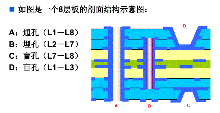
With the increasing speed and miniaturization of mobile phones, notebook computers and other information products, the integration of semiconductor integrated circuits has been continuously improved, and the speed has been continuously accelerated, so the technical requirements for printed boards are higher. The wires on the printed board are thinner and narrower, the wiring density is higher and higher, and the holes on the printed board are smaller and smaller. Using laser blind hole as the main micro-via hole is one of the key technologies of HDI. The characteristics of small aperture and large number of laser blind holes are an effective way to realize high wiring density of HDI board. Because there are many laser blind holes as contact points in HDI board, the reliability of laser blind holes directly determines the reliability of products.
03 Method for judging the reliability of blind holesSo what kind of blind hole is good? We can judge from the following two aspects.
First, the pass pass is generally divided into: plane pass and cross-sectional face type.
(1) Plane pass is mainly judged by roundness index.
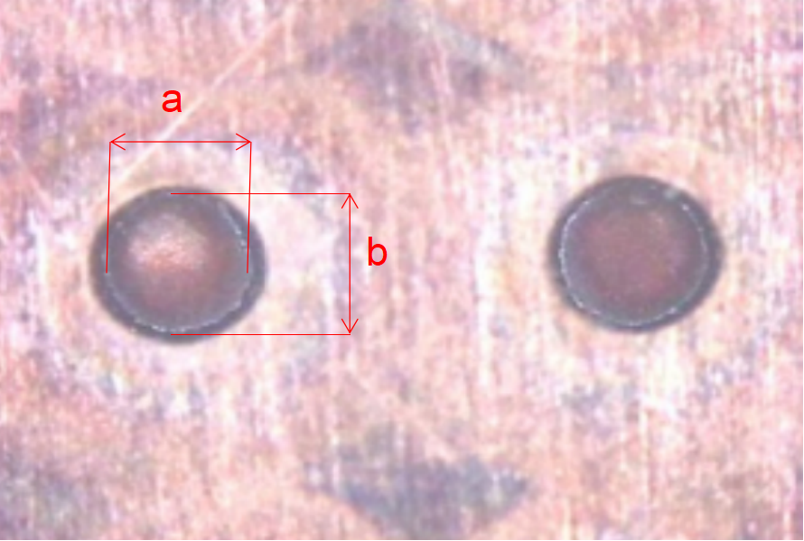
Roundness = short diameter a/ long diameter b*100% In general, roundness is required to be ≥90%, but it will be adjusted according to the actual situation.
(2) For the cross-sectional surface, destructive tests must be carried out, and the slices must be cut and observed. The main indicators are taper, hole wall roughness, copper damage degree of the base material, etc.
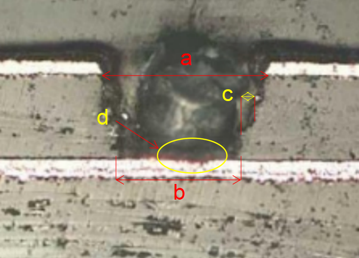
① Taper = lower aperture b/ upper aperture a*100% Under normal circumstances, the taper will be required to be ≥85%, but it will be adjusted according to the actual situation.
② Roughness c of hole wall Generally, blind holes will be required to be ≤15μm, but it may actually be different according to different materials.
③ The damage degree of copper in the base material D In general, the thickness of copper in the base material is required to be ≤1/3, but it will be adjusted according to the actual situation. Note: The grinding of chips may lead to the change of pass, so these items are usually confirmed by taking chips after copper plating.
Second, the copper plating status The key indicators to measure the copper plating status are: corner copper thickness, hole wall copper thickness, hole filling height (bottom copper thickness), dimple value, etc.
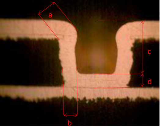
① The copper thickness a at the corner mainly represents the thinnest copper plating point. Because the measuring points and methods are not uniform in the industry, there is no clear standard for the time being. ② The copper thickness of the hole wall is b, which is similar to the copper of the through hole. If the hole is not filled, the through hole standard is generally followed. If the hole is filled, there are many influencing factors, and there is no unified standard in the industry. ③ The hole filling height (bottom copper thickness) d is similar to the surface copper thickness of the through hole, which can be compared with the surface copper standard of the through hole to some extent. ④dimple value c refers to the sag value after hole filling. Only hole filling electroplating has the requirement of dimple value, and the process is difficult, and the general requirement in the industry is ≤ 15 μ m..
The above is about how to judge the reliability of blind holes. The manufacturing process of HDI board is complicated and complicated. When manufacturing, we should first choose the process flow, make clear the key technology of manufacturing, and control the aperture and pass. Reasonable proportion of electroplating solution components; Pay attention to the filling rate and sag to ensure the hole filling effect.
the technology for MULTILAYER PCB and HDI PCB BOARD.
About MaxipcbMaxipcb inspires and empowers innovators and helps them bring world-changing technologies to life. We provide advanced design, simulation and testing solutions to help engineers complete development and deployment faster in the whole product life cycle, while controlling risks. Our customers are all over the world, such as communication, industrial automation, aerospace and national defense, automobile, semiconductor and general electronics. We join hands with customers to accelerate innovation and create a safe and interconnected world. 
