PCB (Printed Circuit Board) is a key electronic component that provides mechanical support and electrical interconnection for electronic devices. It is called a “printed” circuit board because it is fabricated using electronic printing technology.
PCB (Printed Circuit Board) is a key electronic component that provides mechanical support and electrical interconnection for electronic devices. It is called a “printed” circuit board because it is fabricated using electronic printing technology.
Functions of PCB
After adopting printed circuit boards, electronic devices avoid manual wiring errors due to board consistency. They enable automatic component insertion/mounting, soldering, and testing, ensuring product quality, improving productivity, reducing costs, and facilitating maintenance.
Classification of PCBs
-
Single-Sided Boards
Components are placed on one side, and conductors on the other. For SMD components, conductors are on the same side; through-hole components are on the opposite side.
-
Double-Sided Boards
Wiring exists on both sides. Proper interlayer connections (vias) are required to use circuits on both sides.
-
Multi-Layer Boards
More single or double-sided wiring layers are used to expand routing area for high-density designs.
10 PCB Heat Dissipation Methods
Heat is generated during electronic device operation. Without timely dissipation, internal temperature rises rapidly, causing component failure and reduced reliability. Effective PCB thermal management is critical.
(1) Heat Dissipation Through the PCB Itself
Common PCB materials include copper-clad glass epoxy, phenolic glass cloth, and paper-based copper-clad laminates. These materials have good electrical and processing properties but poor thermal conductivity.
Heat is mostly dissipated from component surfaces to ambient air. With miniaturization, high-density mounting, and high-power assembly, surface-only cooling is insufficient.
Heat from SMD components (QFP, BGA) transfers heavily to the PCB. Improvements:
- Add thermal copper foil and use large-area power/ground copper planes
- Apply thermal vias
- Expose copper on the back of IC packages to reduce thermal resistance between copper and air
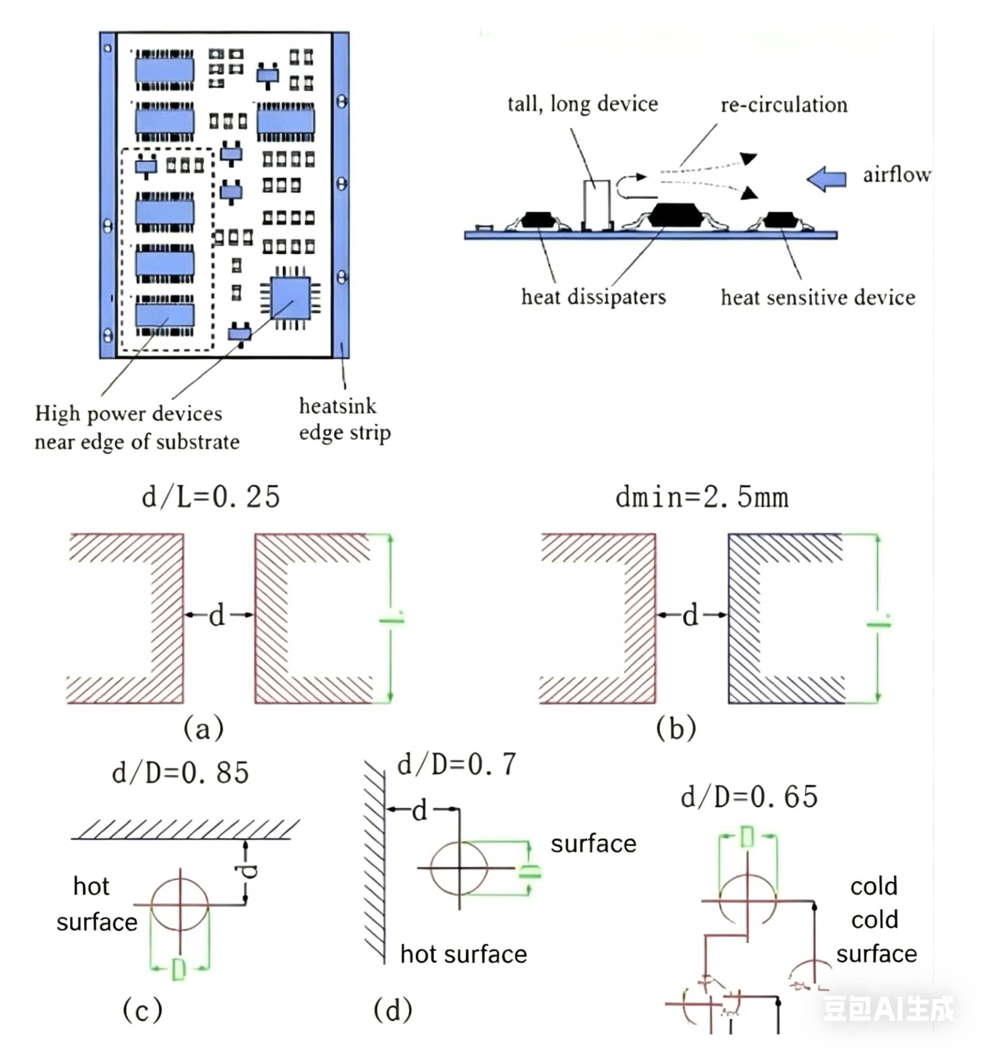
PCB Layout Guidelines
a. Place temperature-sensitive devices in cold-air zones.
b. Position temperature-sensing components at hot spots.
c. Group devices by heat generation: low-power/heat-sensitive devices upstream of cooling airflow; high-power/heat-tolerant devices downstream.
d. Horizontally, place high-power devices near board edges to shorten heat paths; vertically, place them near the top to minimize thermal impact on others.
e. Optimize airflow paths; avoid large empty areas that disrupt natural convection. Apply the same logic to multi-board systems.
f. Mount temperature-sensitive devices in the coolest zones (e.g., device bottom) and not directly above heat sources; stagger components horizontally.
g. Locate high-power/high-heat devices near optimal cooling positions; avoid board corners/edges without auxiliary cooling. Use larger power resistors and reserve sufficient cooling space.
h. Recommended component spacing:
(2) Add Heat Sinks or Thermal Plates for High-Power Devices
For ≤3 high-heat devices: attach a heat sink or heat pipe; add a fan if needed.
For >3 high-heat devices: use a custom large heat shield/plate matched to component heights.
Use soft thermal interface pads to compensate for height differences and improve thermal contact.
(3) Align ICs (and other devices) lengthwise for free-convection cooling
For naturally cooled equipment, arrange integrated circuits in either longitudinal or transverse alignment to enhance airflow.
(4) Heat Dissipation via Optimized Routing Design
Resin has low thermal conductivity; copper traces and vias are excellent conductors.
Key methods: increase copper coverage and add thermal vias.
Evaluate thermal performance using the equivalent thermal conductivity (λeq) of the composite PCB dielectric material.
(5) Group devices by heat generation on the same board
Low-power/heat-sensitive devices (small-signal transistors, small-scale ICs, electrolytic capacitors) upstream; high-power/heat-tolerant devices (power transistors, large-scale ICs) downstream in cooling airflow.
(6) Position high-power devices near board edges (horizontal) and top (vertical)
Shorten heat conduction paths and reduce mutual thermal interference.
(7) Optimize airflow and component placement
Design around natural airflow; avoid large blank areas that block convection. Maintain consistent rules across multiple PCBs in a system.
(8) Protect temperature-sensitive devices
Place them in the coolest areas, not above heat-generating components; use staggered horizontal layout.
(9) Locate high-power devices near optimal cooling points
Avoid board corners/edges without heat sinks. Use appropriately sized power resistors and reserve thermal space.
(10) Avoid hot spots; distribute power evenly across the PCB
Prevent localized high power density that causes overheating and functional failure. Even temperature distribution maintains stable performance.
About Maxipcb
Maxipcb empowers innovators to turn cutting-edge technologies into reality.
We offer one-stop solutions for design, simulation, testing, PCB manufacturing, component procurement and SMT assembly, enabling efficient development, rapid deployment and risk control across the full product lifecycle.Serving the world in communications, industrial automation, aerospace, automotive, semiconductor and beyond, we build a safer, more connected future together.

