The high temperature rise of power chip is a headache for many engineers and friends, among which PCB heat dissipation optimization is an important way to reduce the temperature rise of chip. Today we will share with you: PCB heat dissipation treatment!
The high temperature rise of power chip is a headache for many engineers and friends, among which PCB heat dissipation optimization is an important way to reduce the temperature rise of chip. Today we will share with you: PCB heat dissipation treatment!
"Energy will neither be produced out of thin air, nor will it disappear out of thin air." This is the famous law of conservation of energy, and so is heat.
The temperature of the chip is a manifestation of heat. If concentrated in a specific narrow space, the temperature will rise; If it is dispersed in a large range, the temperature will decrease.
Therefore, to optimize PCB heat dissipation, we must first understand two points:
1. Where is the heat generated?2. How does the heat dissipate?The heat of the chip is mainly generated on the internal wafer, and there are two main ways to conduct the heat:
The first type is wafer-> resin package-> diffused into the air by air convection:
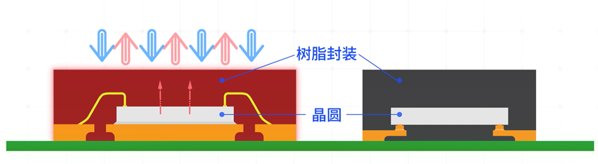
Figure 1: First heat conduction path
The second is that the wafer-> metal pin or heat conducting block ->PCB-> diffuses into the air:
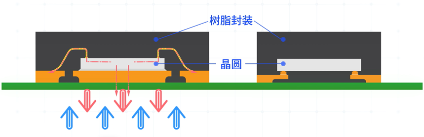
Figure 2: Second heat conduction path
Inside the IC, because the thermal conductivity of metal is much greater than that of resin package, most of the heat is transferred to the outside of the package through metal pins or thermal blocks.
To optimize the heat dissipation of PCB layout, we can adopt the following methods:
1. At the beginning of PCB layout, avoid multiple heat sources (such as multiple power chips, power MOS, MCU with high power consumption, etc.) concentrated in the whole PCB board, which will inevitably lead to local superposition of heat. There should be a certain space between the heating sources to make the heat dissipation of the whole PCB more uniform.
2. When drawing the device package pin pads, we should follow the recommended pad design rules, leaving more than the chip pin area.
This is because if the area of the package lead pad is small, after soldering, the contact area between the solder and the lead and PCB is small, the heat conduction effect is not good, and it is easy to solder. If the appropriate area of the package lead pad is left large, after soldering, the solder has a larger contact area with the lead and PCB board, and the heat conduction effect is better.


Figure 3: Increase the area of package lead pad and optimize the heat conduction effect.
3. In order to increase the heat dissipation of PCB, the copper laying area of power line and ground wire can be increased, and the heat can be transferred quickly through the larger copper laying area, as shown in the figure:
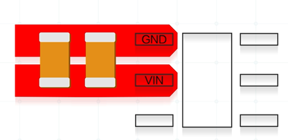
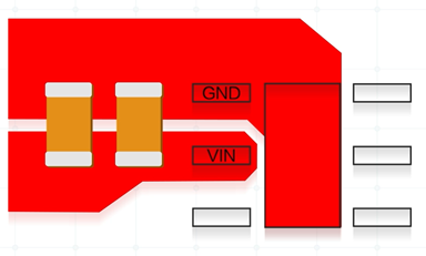
Figure 4: Increase the copper laying area of power line and ground wire.
4. If the PCB process is optional, increasing the copper thickness can have a larger cross-sectional area and enhance the thermal conductivity of PCB wiring.
5. Different layers of PCB have different copper thickness and different thermal conductivity.For multilayer boards, the top and bottom layers are generally 1oz (ounce) thick and the middle layer is 0.5oz thick, so the thermal conductivity of copper between the top and bottom layers is higher than that of the middle layer. And because the top and bottom copper foils are closer to the air, it is easier to radiate heat.
If the middle layer is used as a large area of copper, the heat transfer needs to pass through the middle copper foil first, and then through the insulating isolation layer and the top and bottom copper foils before it can be dissipated into the air, so the heat is naturally not easy to disperse, which leads to the high temperature of the chip. Therefore, the strategy of copper laying for ground wire is very important.
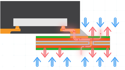
Figure 5: Large-area copper laying on the top and bottom layers is more conducive to heat dissipation.
6. Increase thermal vias. Generally speaking, the more the number of thermal vias, the better the thermal conductivity, and the larger the diameter of thermal vias, the better the thermal conductivity. Therefore, increasing the number and diameter of thermal vias in a reasonable range is helpful to heat conduction.
Generally, the thermal vias are evenly placed under the thermal conductive pad or chip or near the power pin, which can conduct heat to the large-area copper foil at the bottom layer more quickly and make the PCB radiate heat more evenly.
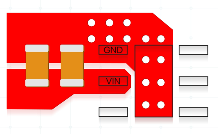
Figure 6: Adding Hot Vias
7. On the premise of ensuring the insulation reliability of the product, solder resist oil can be forbidden to be laid on the bottom layer directly below the IC or at the bottom layer of the thermal via, so as to reduce the thermal resistance between the copper skin and the air in the form of bare copper, and achieve better heat dissipation effect.
Let's look at a comparative example.
DCDC power supply chip MPQ8633B, using four layers of PCB, improves PCB layout design under the condition that the device positions are consistent;
Increase the contact surface of pins, increase the copper laying of power traces, change the ground laying from the middle layer to the top and bottom layers, increase the number and diameter of heat conduction holes, and bare copper at the bottom.
Under the same ambient temperature of 25℃, the IC surface temperatures of the two PCB layout are 101℃ and 74℃ after 10 minutes with the same full load.
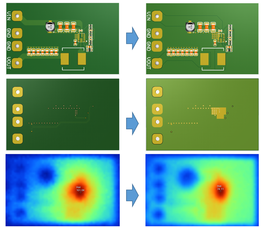
Figure 7: MPQ8633b Comparative Example Diagram
Let's summarize the skills of PCB heat dissipation:
1. Leave heat dissipation intervals between heating sources to avoid centralized placement;
2. The lead pad should be slightly larger than the lead area to ensure the heat conduction area of tin;
3. The top and bottom layers are preferred as power traces or ground layers, and the copper laying area is increased to assist heat dissipation;
4. If the process is optional, the copper thickness can be increased;
5. Add thermal vias, and use the ground at the bottom of PCB to dissipate heat. If necessary, bare copper can be added.
About Maxipcb
Maxipcb empowers innovators to turn cutting-edge technologies into reality.
We offer one-stop solutions for design, simulation, testing, PCB manufacturing, component procurement and SMT assembly, enabling efficient development, rapid deployment and risk control across the full product lifecycle.
Serving the world in communications, industrial automation, aerospace, automotive, semiconductor and beyond, we build a safer, more connected future together.

