1. Cracking Caused by Excessive Coating Thickness
2. Cracking Caused by Flux Residue
How to Solve Cracking
- Optimize the reflow profile; avoid excessively high temperature.
- Ensure the coating is fully cured to achieve optimal performance.
- Reduce the coating thickness.
- Clean the board, especially around solder joints.
3. Delamination on Components
4. Delamination on Solder Mask
Compatibility Between Solder Mask and Conformal Coating
Solder mask contains additives to improve surface quality (appearance, wear resistance, wettability, etc.). These additives may affect the compatibility with conformal coating.
5. Delamination Caused by Masking Removal
Delamination occurs when removing masking due to poor coating adhesion.
Recommendation: Remove masking when the coating reaches
touch dry (still soft).
How to Eliminate Delamination
- Reduce coating thickness.
- Slow down the heating rate in curing.
- Clean the PCB thoroughly.
- Apply a primer to improve adhesion.
6. Two Types of Contamination: Ionic and Non-Ionic
Common sources:
- Mold release agent contamination
- Flux residue
- Fingerprints
7. Defects Caused by Contamination
Coating peeling, coating dissolution or cracking, solder joint corrosion.
8. Chronic De-Wetting
Causes
- Large-area contamination.
- Silicone-containing surfactants in solder mask.
- Silicone-containing adhesives.
- Contaminated cleaning tanks.
- Contamination from HASL (Hot Air Solder Leveling).
9. Local De-Wetting (Type 1)
Solutions
- Wear gloves when handling boards.
- Clean the PCB.
- Solvent-based conformal coatings are less prone to de-wetting than water-based or 100% solid coatings.
10. Local De-Wetting (Type 2)
Causes
- Insufficient coating thickness.
- Excessive thinner.
- Low surface energy of the PCB.
Solutions
- Clean the PCB.
- Use higher-viscosity conformal coating.
11. Pinholes
Causes
- Dust or dirt on the board surface.
- Often caused by manual spraying.
Solutions
- Clean the PCB.
- Water-based coatings are more prone to pinholes.
- Use solvent-based conformal coating.
Where Does Contamination Come From?
- PCB manufacturing process
- Components
- Assembly equipment
- Soldering process
- Operator handling
- Improper cleaning
Corrective Actions
- Clean the PCB.
- For non-cleanable boards, use solvent-based conformal coating.
- Contaminated boards are more likely to have defects with water-based or 100% solid coatings (higher surface tension).
12. Capillary Phenomenon
Capillary phenomenon in conformal coating
Causes
- PCB design: connectors with fine-pitch pins.
- Overly strict coating requirements.
- Conformal coating viscosity too low.
- Excessive coating flow rate.
- Mismatched surface tension between substrate and coating.
Solutions
- Increase distance between coated area and connectors.
- Use masking tape to form a dam around connectors.
- Use higher-viscosity conformal coating.
- Reduce coating thickness.
- Clean the PCB.
Common Bubble Types
- Large bubbles: diameter > 300 μm
- Small bubbles: diameter < 300 μm
- Mixed large and small bubbles
How to Solve Bubbles
Key factors to check:
- Full coating line process
- Conformal coating type
- Coating viscosity and thickness
- Coating equipment
- Curing equipment
- PCB design
Typical Solvent-Based Coating Line
Selective coater → leveling & solvent evaporation conveyor → 4 m IR curing oven (1 m UV oven for UV cure)
Solvent Evaporation / IR Curing
Solvent evaporation accelerates with temperature.
Bubbles form when:
- Excess solvent trapped in the film
- Oven temperature too high (skin forms rapidly)
- Coating viscosity too high to release bubbles
- Coating too thick to release bubbles
- Exhaust too high or too low in the leveling zone
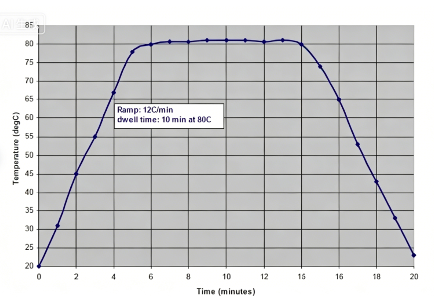
A proper thermal profile is critical.
[ILLUSTRATION 2] Typical curing temperature profile for solvent-based conformal coating
- Ramp: 12 °C/min
- Dwell: 10 min at 80 °C
Diagnostic Test
- Board 1: runs full process
- Board 2: air dries at room temperature
Compare after surface dry:
- Bubbles only on Board 1: caused during curing
- Bubbles on both: caused during coating
- Bubbles only on Board 2: not observed
Bubble Solutions
- Large bubbles (solvent boiling)
Optimize thermal profile (slower ramp), increase pre-cure leveling, reduce coating volume and overlap.
- Small bubbles (compressed air spray)
Lower spray pressure, lower curing temperature, increase leveling time, change thinner type.
13. Bubbles in UV Conformal Coating
Bubbles in UV coating = foam.
Most UV coatings are solvent-free or low-solvent, but leveling is still necessary.
Recommendations:
- Avoid compressed-air spray and atomization; use diaphragm pumps.
- Let the coating stand for 1 hour after filling.
14. Orange Peel
Caused by forced drying/curing.
Solutions
- Check environmental conditions (temperature, humidity).
- Compare room-temperature-cured vs. process-cured boards.
- Reduce exhaust in the pre-cure leveling zone.
- Lower coating viscosity.
- Slow down the thermal profile ramp rate.
- Use slower-evaporating thinner.
About Maxipcb
Maxipcb empowers innovators to turn cutting-edge technologies into reality.
We offer one-stop solutions for design, simulation, testing, PCB manufacturing, component procurement and SMT assembly, enabling efficient development, rapid deployment and risk control across the full product lifecycle.Serving the world in communications, industrial automation, aerospace, automotive, semiconductor and beyond, we build a safer, more connected future together.

