Hardware engineers new to multi‑layer PCB design often feel confused when facing 8‑layer, 10‑layer or higher boards with dense, web‑like routing.
Hardware engineers new to multi‑layer PCB design often feel confused when facing 8‑layer, 10‑layer or higher boards with dense, web‑like routing.
This article presents 3D internal structure diagrams of multi‑layer PCBs to clearly show different stack‑up architectures.
01 Core of HDI Boards: Vias
The trace fabrication of multi‑layer PCBs is similar to single‑ and double‑layer boards. The biggest difference lies in
via processes.
Traces are etched; vias are drilled and copper‑plated.
Multi‑layer boards are mainly classified into:
- Through‑hole boards
- 1st‑order HDI
- 2nd‑order HDI
- 2nd‑order stacked via HDI
Higher‑order types (3rd‑order, Any‑Layer Interconnect (ALIVH)) are rarely used and very expensive, so they are not covered here.
Typical applications:
- 8‑bit MCUs: 2‑layer through‑hole
- 32‑bit MCU smart hardware: 4–6‑layer through‑hole
- Linux/Android devices: 6‑layer through‑hole to 8‑layer 1st‑order HDI
- Smartphones: 8‑layer 1st‑order to 10‑layer 2nd‑order HDI
8‑layer 2nd‑order stacked via HDI (for Qualcomm Snapdragon 624)
02 Most Common: Through‑hole Boards
A
through‑hole board uses only one type of via: drilled from the top layer to the bottom layer, fully penetrating the board.
Through‑holes are not related to layer count. 2‑layer boards are all through‑hole; even 20‑layer telecom or military boards can still be through‑hole.
Vias are mechanically drilled through the board, then copper‑plated to form conduction paths.
Notes:
Common finished via diameters: 0.2 mm, 0.25 mm, 0.3 mm.
0.2 mm vias are much more expensive than 0.3 mm because tiny drills break easily and drill slowly.
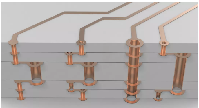
03 HDI Boards: Laser Drilled Vias
6‑Layer 1st‑Order HDI Board
- Layers 1–2: laser vias (0.1 mm diameter)
- Layers 2–5: mechanical through‑holes
- Layers 5–6: laser vias
This structure is equivalent to a 4‑layer through‑hole board with two additional outer layers.
Laser can only drill fiberglass dielectric, not copper, so outer laser drilling does not affect inner traces.
After laser drilling, copper plating forms laser vias.
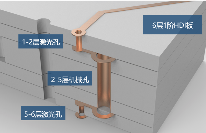
6‑layer 1st‑order HDI stack‑up structure
04 2nd‑Order HDI: Two Stages of Laser Vias (Staggered)
6‑Layer 2nd‑Order Staggered HDI Board
- Layers 1–2: laser vias
- Layers 2–3: laser vias
- Layers 3–4: mechanical vias
- Layers 4–5: laser vias
- Layers 5–6: laser vias
2nd‑order: two stages of laser vias.
Staggered: laser vias in adjacent stages are offset.
Reason: copper plating cannot fully fill narrow vias, so stacked drilling is not allowed.
Rules:
- 6‑layer 2nd‑order = 4‑layer 1st‑order + 2 outer layers
- 8‑layer 2nd‑order = 6‑layer 1st‑order + 2 outer layers
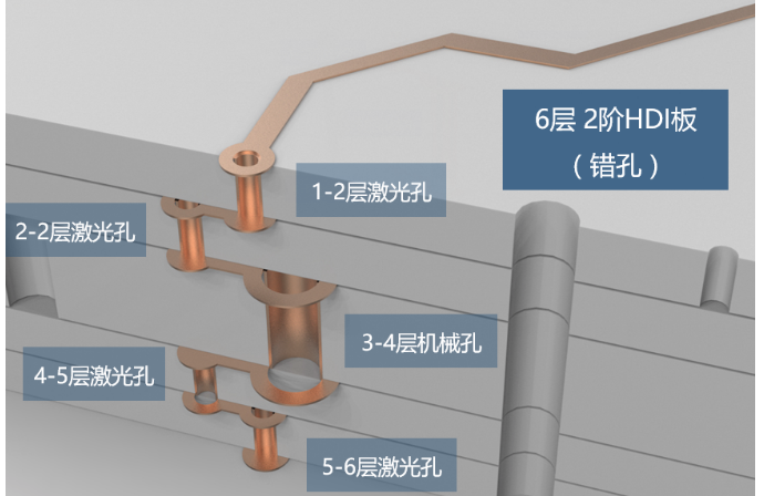
6‑layer 2nd‑order staggered HDI structure
05 Stacked Via HDI: Complex and Costly
6‑Layer 2nd‑Order Stacked Via HDI Board
Laser vias between layers 1–2 and 2–3 are
vertically aligned (stacked).
This allows more compact routing.
Requirement: inner laser vias must be fully copper‑plated and filled before outer laser drilling.
Price is higher than staggered via boards.
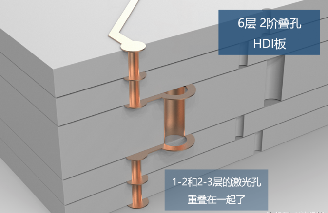
6‑layer 2nd‑order stacked via HDI structure
06 Premium Any‑Layer Interconnect (ALIVH) Boards
Every layer uses laser vias, and any layer can connect to any other layer.
Great for layout engineers, but cost is
more than 10× that of standard through‑hole boards.
Only used in high‑end products like iPhone.
Summary
Compare via size and whether via pads are closed or open.
Comparative summary diagram of via types and pad styles
About Maxipcb
Maxipcb empowers innovators to turn cutting-edge technologies into reality.
We offer one-stop solutions for design, simulation, testing, PCB manufacturing, component procurement and SMT assembly, enabling efficient development, rapid deployment and risk control across the full product lifecycle.Serving the world in communications, industrial automation, aerospace, automotive, semiconductor and beyond, we build a safer, more connected future together.


