For multi-layer PCB design, the layer stackup of the PCB is an extremely critical step. The quality of the layer stackup has a direct impact on product performance. Below we summarize the basic principles of multi-layer board layer stackup.
For multi-layer PCB design, the layer stackup of the PCB is an extremely critical step. The quality of the layer stackup has a direct impact on product performance. Below we summarize the basic principles of multi-layer board layer stackup.
First, signal layers shall be stacked adjacent to ground layers. With adjacent ground layers, crosstalk and electromagnetic radiation between signals can be effectively reduced. Ground layers can provide current return paths and shield electromagnetic radiation from signal layers. Especially in high-frequency and high-speed PCB design, adjacent ground layers can also avoid signal cross-division issues. Therefore, in PCB design, critical signals shall also be placed in signal layers close to ground layers.
[Table 1: 12-layer PCB stackup structure parameters]
Second, layer stackup symmetry shall be maintained during stacking. The symmetry of the layer stackup is related to the warpage of the finished PCB in the later stage. Asymmetric layer stackup will cause warpage of the finished board, further affecting the SMT assembly of the board, and may lead to poor soldering, cold soldering and other issues.
Third, the layer adjacent to components shall be set as a ground plane, which can provide shielding for devices and avoid cross-division of signals on the top and bottom layers (cross-division means that the adjacent reference layer of a signal passes through multiple planes).
Fourth, power planes shall be adjacent to ground planes as much as possible to form a planar capacitor, thereby reducing the impedance of the power plane.
[Table 2: 4-layer PCB stackup structure parameters]
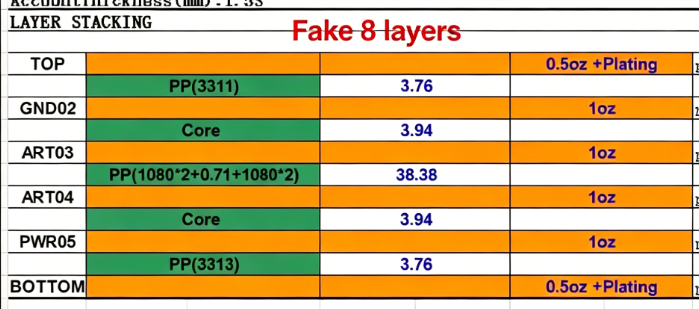
Fifth, adjacent parallel routing layers shall be avoided as much as possible. The crosstalk between adjacent parallel routing layers will be very large, thereby affecting signal quality and board performance. If adjacent routing layers are unavoidable, route horizontally on one layer and vertically on the other, or increase the thickness between these two layers to widen the spacing, which can effectively solve the crosstalk problem, such as the commonly referred to as "false 8-layer" design.
[Table 3: False 8-layer PCB stackup structure parameters]
 About Maxipcb
Maxipcb enables advanced electronic innovation. We deliver one-stop solutions including circuit design, simulation, testing, PCB fabrication, component sourcing and SMT&PCBA assembly, to boost R&D efficiency, speed up mass production and control full-cycle risks. We serve global sectors like communication, industrial automation, aerospace, automotive and semiconductor, jointly forging a safer, connected intelligent future.


