DC-DC converters enable efficient power conversion and power supply at various voltage levels. However, with rising demands for higher power density, higher efficiency, and smaller form factors, PCB design for DC-DC conversion has become increasingly critical.
DC-DC converters enable efficient power conversion and power supply at various voltage levels. However, with rising demands for higher power density, higher efficiency, and smaller form factors, PCB design for DC-DC conversion has become increasingly critical.
This article mainly analyzes DC-DC conversion component selection, minimum EMI layout, and thermal management.
1. Routing Considerations
PCB routing of DC-DC converters significantly affects electromagnetic interference levels. Proper PCB routing techniques help minimize EMI. Trace length and loop area are key factors in PCB design for DC-DC converters, especially high-frequency switching converters.
1.1 Trace Length
In high-frequency converters, the length of traces carrying high-speed switching signals is critical for maintaining signal integrity and reducing EMI. Long traces can act as antennas and radiate electromagnetic energy, potentially interfering with other components or circuits. In addition, long traces can cause delay, signal reflection, and parasitic effects, leading to reduced converter efficiency and stability. Therefore, trace lengths should be as short as possible, especially for high-speed clocks and data clocks. Proper impedance matching techniques and controlled-impedance traces can further optimize signal transmission and minimize signal attenuation. For high-speed signals, it is important that the trace lengths of differential pairs are identical across the entire PCB; if mismatched, meander traces should be implemented near the mismatched edges.
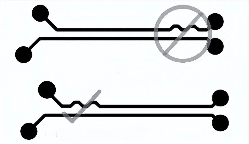
Differential Pair Trace Matching for Gate Signals in High-Speed DC-DC Converters
1.2 Loop Area
Loop area refers to the enclosed area formed by signal traces and their return paths on a PCB. In high-power and high-frequency circuits such as DC-DC converters, minimizing loop area is critical for reducing radiated EMI. A larger loop area results in greater magnetic flux coupling into the loop, leading to higher EMI. The primary measure to minimize loop area is to place signal traces close to their return paths (e.g., using ground planes / closely spaced power planes).
2. Filter Components
Adding filter components such as ferrite beads and common-mode chokes to critical signal and power lines attenuates conducted electromagnetic interference and prevents further propagation. Proper placement is essential for filtering EMI when connecting filter capacitors.
Filter components should be placed as close as possible to the DC-DC converter. Proper placement of decoupling capacitors near the power pins of ICs and active components helps suppress high-frequency noise and improve EMI performance.
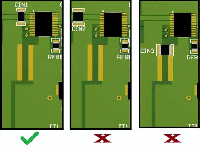
Decouple Capacitor Placement in DC-DC Converters
3. Parasitic Inductance and Capacitance
3.1 Path Inductance
Path inductance is the inherent inductance of a conductive path (e.g., trace/wire), dependent on its physical dimensions and material properties. In high-frequency circuits such as DC-DC converters, path inductance affects converter efficiency and performance.
High path inductance causes voltage drop, increased switching losses, reduced converter efficiency, and may lead to voltage overshoot and ringing in the circuit, impairing signal integrity. To minimize path inductance, PCB engineers can use wider traces, shorter paths, or dedicated ground/power planes to create low-inductance return paths for high-current/switching signals.
3.2 Stray Capacitance
In high-frequency circuits, stray capacitance couples with high-speed signals, causing unwanted capacitive coupling, increased EMI, and potential signal distortion and degradation. To minimize stray capacitance, proper spacing should be maintained between signal traces, ground planes, and power planes. Appropriate ground segmentation and isolation also help reduce parasitic capacitance.
4. Impact of Ground Loops in DC-DC Converters
When designing DC-DC converters, PCB engineers must account for current loops and properly place components to physically minimize loop sizes.
4.1 Effects of Excessively Long Ground Loops
Excessively long ground loops cause the following issues:
- Electromagnetic Interference: Ground loops act as antennas, radiating EMI into the surrounding environment.
- Noise and Signal Attenuation: Current flowing through ground loops creates voltage differences between ground points, potentially introducing unwanted noise into sensitive signal paths, causing signal attenuation and reduced signal-to-noise ratio.
- Common-Mode Noise: Ground loops can couple common-mode noise into sensitive analog or digital circuits, degrading signal accuracy—especially in low-level analog measurements or high-speed digital communications.
- Parasitic Ground Current: Circulating current flows between different ground points, creating parasitic ground current. Parasitic current generates voltage drops, degrades converter performance, and causes low efficiency and potential thermal issues.
- Ground Bounce: Ground loops create voltage differences between ground reference planes, causing ground bounce. Ground bounce is a transient increase in ground voltage during switching events, which impairs signal integrity and disrupts normal digital circuit operation.
4.2 Ground Loop Mitigation Measures
- Star Grounding: Concentrate all ground points to a single reference point to eliminate ground loops and reduce ground-related issues.
- Ground Planes: Use solid ground planes on the PCB to ensure low-impedance return paths for current, reducing ground loop risk.
- Ground Segmentation: Properly split ground planes for different functional blocks or components to prevent mutual interference of ground currents.
- Isolate Analog and Digital Grounds: Physically separate analog and digital ground planes to prevent interference between sensitive analog circuits and noisy digital circuits.
- Trace Routing: Ensure traces carrying high-current or high-frequency signals have low-inductance return paths (e.g., short, wide traces or ground vias) to minimize ground loop formation.
5. Layer Stackup
Layer stackup refers to the arrangement and configuration of conductive and dielectric layers that constitute a PCB. It is critical for determining board performance, functionality, and manufacturability. The importance of layer stackup is analyzed below:
5.1 Signal Integrity and EMI Control
Careful placement of signal layers and ground/power planes ensures controlled impedance for high-speed signals, reduces crosstalk, and improves noise immunity.
5.2 Grounding and Power Distribution
Layer stackup enables proper distribution of ground and power planes across the PCB. Ground planes provide low-impedance return paths for signals, minimizing ground bounce and noise. Adequate power distribution ensures efficient power delivery, reducing voltage drop and power loss.
5.3 Thermal Management
Layer stackup affects PCB thermal performance. By assigning dedicated copper layers for power and ground planes and carefully placing thermal vias, engineers effectively dissipate heat generated by power components and ensure proper thermal management.
5.4 Manufacturability and Assembly
Correct layer arrangement, drill alignment, and clear stackup specifications enable smooth manufacturing and assembly, reducing the risk of defects and errors in production.
5.5 Multi-Layer Design and Miniaturization
Layer stackup allows engineers to design compact and miniaturized PCBs.
5.6 EMC Compliance
Layer stackup helps manage signal return paths, minimize loop area, and reduce EMI, supporting PCB compliance with EMC regulations.
5.7 Signal Routing and Partitioning
Layer stackup enables efficient signal routing and partitioning between functional blocks on the PCB. Isolating sensitive analog, digital, and power circuits on separate layers enhances signal isolation and reduces interference.
6. Trace Sizing for DC-DC Converter PCBs
Trace width requires careful consideration, as it directly affects PCB current-carrying capacity, power loss, and thermal performance. Key factors for determining PCB trace width are listed below:
6.1 Current-Carrying Capacity
Determine the maximum current carried by each trace in the DC-DC converter circuit, including current through power components (MOSFETs, inductors, capacitors) and high-current signal traces. The maximum current shall account for transient spikes and potential overcurrent conditions.
6.2 Temperature Rise and Allowable Temperature
Calculate trace temperature rise from maximum current and trace width using the formula:
ΔT = (I² × R_trace) / (k × A)
- ΔT: Temperature rise
- I: Current
- R_trace: Trace resistance
- A: Cross-sectional area of the trace
- k: Thermal constant of the PCB material
6.3 Trace Resistance
Calculate trace resistance using the formula:
R_trace = ρ × (L / A)
- ρ: Resistivity of trace material (copper)
- L: Trace length
- A: Cross-sectional area of the trace (width × thickness)
6.4 Voltage Drop
Calculate the acceptable voltage drop across the trace based on the maximum current and allowable voltage drop specified in design requirements.
6.5 Copper Weight and Thickness
Determine PCB copper weight and thickness. Standard copper weights include 1 oz (35 µm), 2 oz (70 µm), and 3 oz (105 µm).
Thicker copper enables higher current-carrying capacity but increases PCB cost and manufacturability considerations.
6.6 Trace Width Calculation
Use calculated current, trace resistance, and voltage drop values to compute the required trace width via online trace width calculators or PCB design software that accounts for PCB copper thickness and material.
6.7 Dimensional Space Constraints
Ensure the determined trace width fits the available area and complies with clearance and spacing requirements.
6.8 Heat Dissipation
Ensure the calculated trace width and copper weight enable efficient heat dissipation without excessive temperature rise, especially for high-current traces.
About Maxipcb
Maxipcb enables advanced electronic innovation. We deliver one-stop solutions including circuit design, simulation, testing, PCB fabrication, component sourcing and SMT&PCBA assembly, to boost R&D efficiency, speed up mass production and control full-cycle risks. We serve global sectors like communication, industrial automation, aerospace, automotive and semiconductor, jointly forging a safer, connected intelligent future.


