the tips for routing impedance‑controlled traces on multilayer PCBs.
Today I’m going to share tips for routing impedance‑controlled traces on multilayer PCBs.
1. What is PCB Impedance?
PCB impedance is the combined effect of capacitance and inductance in a circuit operating at high frequencies. Measured in ohms (Ω), it differs from DC resistance: impedance is an AC characteristic dependent on frequency, while resistance is not.
2. The Importance of Impedance for PCBs
Impedance matching is mandatory for high‑speed data transmission on PCBs.
Take the USB interface in mobile phones as an example: it supports bidirectional synchronous data transfer, high speed, and low cost. Common types include Type A, Type B, and Type C.
The USB protocol defines differential signal pairs such as (D+, D−), (TX+, TX−), and (RX+, RX−) for digital signal transmission. To ensure stable signal transmission, differential traces on a PCB must follow strict differential routing rules.
3. Key Notes for Impedance Routing on Multilayer PCBs
-
Place component pads as close together as possible to shorten the distance between pads, keep differential traces as short as possible, and minimize the number of vias.
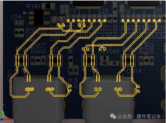
Components placed with pads close together
-
Traces must be parallel and symmetric. Avoid 90° bends; use
45° angles or curved arcs instead. Maintain trace spacing within
4 mils.
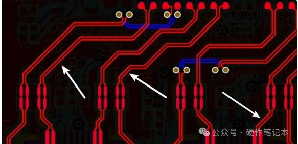
45° or arc routing for differential pairs
-
When placing series resistors and capacitors, align them vertically or horizontally.
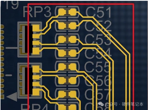
Vertical or horizontal alignment of series R/C components
-
Differential impedance traces should maintain equal length and equal spacing to avoid timing skew and common‑mode interference.
Equal‑length, equal‑spacing differential impedance traces
-
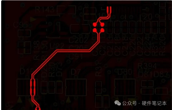
Due to pin arrangement, vias, routing space, and other factors, differential trace lengths often become mismatched. Length mismatch causes timing skew and degrades signal quality.
Compensate for length mismatch in differential pairs to equalize trace lengths. The length difference is typically controlled within
5 mils. The compensation rule is to correct the section where the length mismatch occurs.
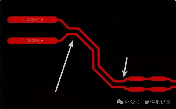
Length compensation for mismatched differential pairs
Example Parameters
- H1: Dielectric thickness (between impedance trace and reference layer)
- ER1: Dielectric constant of the substrate: 4.2–4.6 (PP: 4.2; core: 4.5)
- W1: Designed trace width
- W2: Top trace width = designed trace width − 0.5 mil
- S1: Spacing between the two traces
- T1: Copper weight, typically 1 oz (1.4 mil)
- C1: Solder mask thickness on substrate surface
- C2: Solder mask thickness on copper surface
- C3: Solder mask thickness on base material surface
- CER: Solder mask dielectric constant: 3.5
Using an impedance calculator with these values yields a target impedance of approximately
100 Ω.
About Maxipcb
Maxipcb empowers innovators to turn cutting-edge technologies into reality.
We offer one-stop solutions for design, simulation, testing, PCB manufacturing, component procurement and SMT assembly, enabling efficient development, rapid deployment and risk control across the full product lifecycle.Serving the world in communications, industrial automation, aerospace, automotive, semiconductor and beyond, we build a safer, more connected future together.


