Design professionals often talk about design-for-manufacturing guidelines, but what exactly are these guidelines and how are they implemented in your PCB design software? In PCB development, design for manufacturing has a very simple meaning: you should only implement a design choice if it ensures maximum manufacturable yield.
By Zachariah Peterson
Design professionals often talk about design-for-manufacturing guidelines, but what exactly are these guidelines and how are they implemented in your PCB design software? In PCB development, design for manufacturing has a very simple meaning: you should only implement a design choice if it ensures maximum manufacturable yield. This seemingly simple explanation leaves out many key points, and it is natural to assume that manufacturers can build anything you place in your PCB layout within the design software.
In reality, different fabrication houses have different capabilities, material selections, and standard non-contact service options. There are some very common mistakes or oversights that can render a board unmanufacturable and may require significant redesign. In this article, I will review some of the most common mistakes that both new and experienced designers can make. I have made these mistakes myself, but I can tell you that you can always recover from them and ensure your boards are manufacturable.
Some Basic DFM Tips for PCB Design
The points I outline below almost exclusively cover two important areas:
- Material considerations, especially core/laminate materials and copper weight
- Manufacturing constraints, especially dimensions and spacing in the PCB layout
With that in mind, let’s dive into some basic PCB design and manufacturing guidelines to ensure design success.
Get the Layer Stack First
You’d be surprised how easy it is to jump straight into a new design and start placing components around the board. For simpler boards that don’t require impedance control, specific bus capacitance, or dense digital routing, you might start laying out on an even-layer board with standard layer thicknesses. Depending on the design, the manufactured PCB may not deliver the functionality you expect.
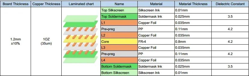
Example of a standard layer stack provided by a PCB fabricator
PCB fabrication houses can send you a stackup table to help ensure your design is manufacturable. For most designs, even hobbyist microcontroller boards, you need to understand at minimum the layer arrangement and material properties. Before you start designing digital bus traces or any impedance-controlled traces, email the fabrication house for a standard layer stack. If you don’t, the fabricator might build your board with a stackup that doesn’t create your intended functionality. Another risk is creating a stackup they cannot manufacture, usually because they don’t have materials in stock that meet your stackup specifications.
Match Copper Weight to Current Density and Laminate
Don’t be surprised if a manufacturer rejects your chosen copper weight when selecting materials or getting an approved stackup. You must use the copper weights available in the manufacturer’s material set; you cannot just specify any copper weight you want. If you’ve taken the time to estimate the required copper weight and trace width for a specific current density (e.g., on power rails), be sure to specify the required weight when finalizing the stackup with the manufacturer.
Enforce Copper-to-Copper Clearance
When you start a new PCB layout, your ECAD software will apply a default set of clearance rules that are conservative for nearly all PCBs. These values are often overly conservative, so they are commonly ignored without programming the correct clearance values before starting layout. Worse, you might enter values that are too small, causing you to place elements too close together for the board to be manufactured.
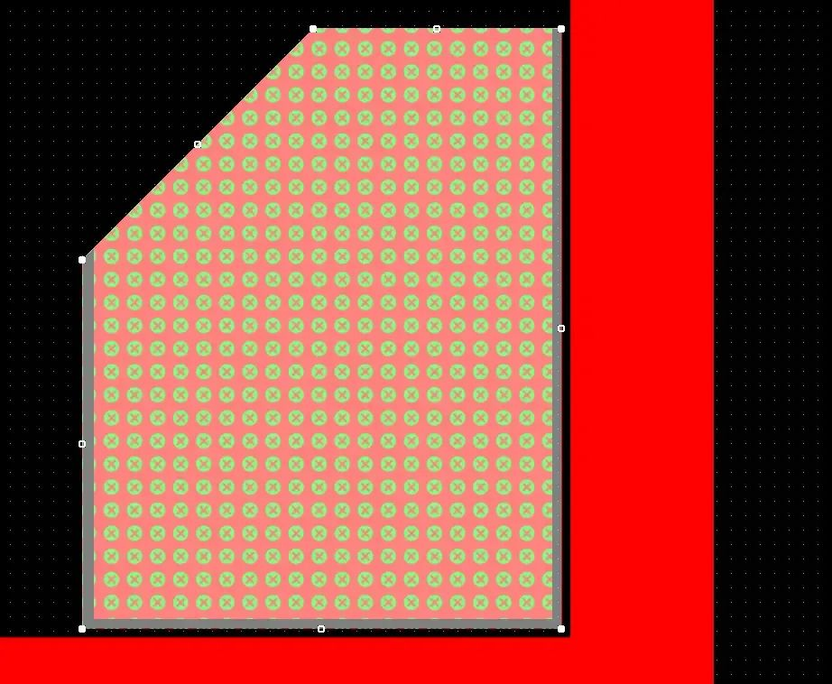
Polygon pour near a trace; DRC engine flags clearance errors along the trace
Note the polygon pour placed near this trace: the DRC engine has marked clearance errors along the trace length in this window. You should set trace-to-pour clearance rules to ensure these elements do not get too close, otherwise you risk unintended shorts between them during manufacturing.
Solution: Get the manufacturer’s constraints before you start placing components, and program these values as design rules into your PCB project. If you want to avoid the most common clearance violations, focus on these clearances:
- Trace-to-trace
- Trace/pad-to-pour
- Trace-to-pad
- Pad-to-pad
The last two apply to SMD pads and landing pads for through-holes (vias or component leads). Note that these values will be larger for heavier copper due to etching compensation requirements.
Overlapping Drill Holes
If you followed the earlier clearance guidelines and set minimum pad spacing values, you may have already addressed this DFM guideline. If drill holes are placed too close together, they can overlap due to shifts in CNC drilling. Each drill hit deviates slightly from its ideal position, and this must be accounted for when placing vias and through-hole leads.
A similar problem can occur between drilled features crossing planes, such as the thermal relief and GND plane clearance shown in the image below. The two green areas show the clearance between the via barrel and the plane for these nets; the remaining copper sliver here is extremely small and unmanufacturable. The specific example shown is a case where such a manufacturing defect would not render the device inoperable, but this is often not the case. If such a defect appears on the surface layer between two through-holes, it creates a risk of bridging during soldering, as narrow copper features can be etched away during manufacturing.
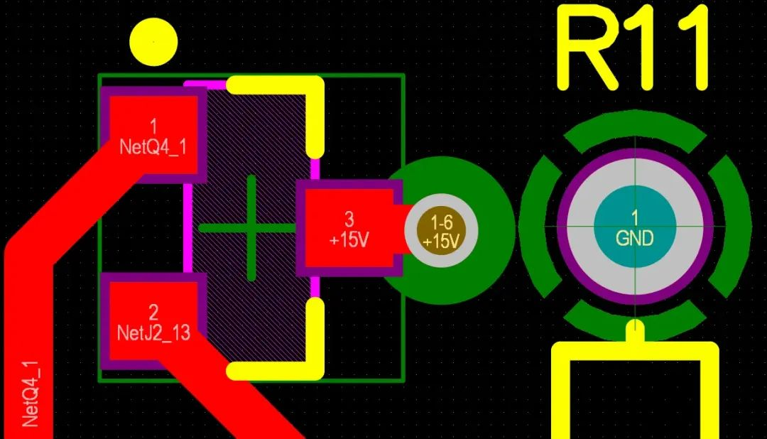
Two closely spaced vias leaving a tiny unmanufacturable copper sliver on an internal plane
The tight spacing between these two vias leaves a very tiny copper sliver on the plane layer that will be over-etched and will not appear on the manufactured board.
The natural solution here is to simply use larger pads, which is what is done to meet basic IPC class requirements: use a minimum pad size (drill diameter) + 8 mils to ensure drill-to-drill clearance limits are almost always satisfied.
Small Feature Sizes
As you start packing components and traces onto a board, it’s easy to begin making traces, drills, and pads too small. Clearance rules already limit how closely you can pack everything, but equally important design requirements are minimum feature sizes. The two most common points you need to address are minimum hole size and trace width. This is as simple as looking up the manufacturer’s feature sizes and programming them into your design rules.
Typical manufacturing limits for most boards are 4-mil trace width and 6-mil drill diameter. For many simple boards that don’t require impedance control, it’s better to use 8–10 mil trace widths and 10-mil drill diameters.
Solder Mask Slivers
This is an often-overlooked aspect of assembly, meant to ensure solder mask openings reliably act as a barrier to prevent molten solder from flowing between nearby components. Even with properly spaced pads, oversized solder mask openings on NSMD pads can leave very thin solder mask webs between pads.

Thin unmanufacturable solder mask sliver between Q9 and Q10 pads
The remaining solder mask sliver between Q9 and Q10 will not be manufacturable because it is too thin. However, the pad-to-pad clearance is still acceptable.
The solution here is to reduce the solder mask openings on these pads to 0 mils. You may also need to increase the spacing between these components by a few mils. A typical minimum solder mask sliver requirement here is 5 mils. When a solder mask sliver falls below the manufacturer’s limit, it can break off after curing and create a channel where two pads can be bridged with solder. The fix is to apply extra spacing or reduce solder mask openings on affected pads so a sufficiently large sliver remains.
Overlapping Silkscreen
Once placement and routing are complete, you should check the silkscreen layer to ensure no reference designators overlap. If they do, you can move them in the PCB layout until everything is legible. While this is not technically required for successful manufacturing or assembly, responsible manufacturers will still flag this as an issue during design review.
A more critical problem is silkscreen overlapping pads/holes where solder will be applied. Be sure to check this using a 3D model viewer or by directly inspecting the Gerber files.
The list of guidelines above should address the most common DFM issues that can affect nearly any design. When you implement these guidelines in your projects, they will become part of your normal design process. Once you have these points programmed into your design rules, you can always check them as part of a design review before sending your boards into production.
About Maxipcb
Maxipcb empowers innovators to turn cutting-edge technologies into reality.
We offer one-stop solutions for design, simulation, testing, PCB manufacturing, component procurement and SMT assembly, enabling efficient development, rapid deployment and risk control across the full product lifecycle.Serving the world in communications, industrial automation, aerospace, automotive, semiconductor and beyond, we build a safer, more connected future together.


