Many friends have sent me private messages asking for a hands-on demonstration. Coincidentally, there is a smart lock project where the card reading distance is only about 3mm, and the reading distance needs to be optimized. This debugging record documents the thinking process during debugging, and comments and corrections are welcome.
Many friends have sent me private messages asking for a hands-on demonstration. Coincidentally, there is a smart lock project where the card reading distance is only about 3mm, and the reading distance needs to be optimized. This debugging record documents the thinking process during debugging, and comments and corrections are welcome.
1. NFC Circuit Schematic and PCB Design
2. Start Debugging
The debugging steps are as follows:
- Determine the optimal operating impedance of the NFC chip
- Design the antenna coil and measure the equivalent circuit parameters of the antenna coil
- Determine the resistance value of series/parallel resistors according to Q factor or bandwidth requirements; in most cases, a series circuit is sufficient, and the parallel circuit is a conversion of the series circuit. This article only explains the series circuit.
- Determine the cutoff frequency of the LC-structured EMC filter according to the high-order harmonic components to be filtered out, and calculate the L and C values of the EMC filter
- Calculate the capacitance values in the impedance transformation circuit to achieve conjugate matching
- Actual testing and parameter adjustment
2.1 Determine the Optimal Operating Impedance of the NFC Chip
The NFC chip used in this debugging project is FM5114B. The impedance of TX1 and TX2 cannot be found in the datasheet. After contacting the FAE by phone, I was informed that the impedance between TX1 and TX2 is about 25Ω, and a reference document was sent, which also requires matching near 25Ω on the Smith chart.
2.2 Design the Antenna Coil and Measure Its Equivalent Circuit Parameters
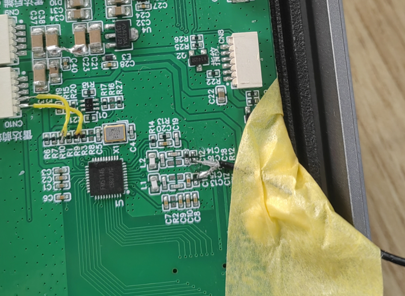
Before measurement, the vector network analyzer must be calibrated and the time delay of the RF feeder compensated. Remove C17 and C18, disconnect C13 and C14, and solder the feeder to the left side of C13 and C14. The test data are as follows:
Test instrument: Lite VNA
Antenna data: 1.92+j80.44Ω
Thus Q = 80.44/1.92 = 41.89
The resistance of this antenna is a bit high! The NFC antenna is connected to the control chip through an interface connector, which may be the reason. The result remains the same after multiple measurements.
The Q factor is about 42, which is acceptable. Whether the bandwidth needs to be adjusted will be determined during the actual reading distance test. The FAE stated that their typical Q factor is about 36. As is often the case, many parameters cannot be found in the datasheet and can only be obtained through communication.
2.3 Calculate L and C Values of the LC Filter
Online LC cutoff frequency calculation:
Resonant frequency: 14.34MHz
Capacitance: 560.0pF, Inductance: 220.0nH
This value is a bit small, and the cutoff frequency of the filter circuit is too high: 13.56+0.007+0.8475=14.4145MHz. Change the capacitance from 560pF to 470pF.
13.56MHz NFC/RFID Operating Bandwidth
|
ISO14443-A |
ISO14443-B |
ISO15693 |
| Operating Frequency |
13.56MHz |
13.56MHz |
13.56MHz |
| Allowable Frequency Deviation |
±7KHz |
±7KHz |
±7KHz |
| Subcarrier Frequency |
847.5kHz |
847.5kHz |
423kHz |
| Data Rate |
106kbps |
106kbps |
27kbps |
| Operating Bandwidth |
1.921MHz |
1.921MHz |
0.924MHz |
2.4 Calculate Capacitance Values in the Impedance Transformation Circuit to Achieve Conjugate Matching
- First test the impedance of the chip and filter circuit
Remove the chip, solder a 23.5Ω resistor (47/2=23.5Ω, no 25Ω resistor available) between TX1 and TX2, disconnect C13 and C14, solder the VNA cable to the right side of C13 and C14, and the measured result is as follows:
Z=55.64-j40.33Ω
-
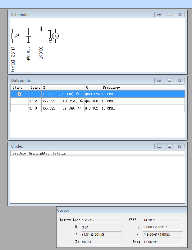
The following is the transformation from the antenna data: 1.92+j80.44Ω to the target impedance after matching: Z=55.6±j40.33Ω (note the series-parallel conversion of components)
-
Simulation with Smith Chart:
First parallel 120pF, then series 30pF
| Start |
Point |
Z |
Q |
Frequency |
|
DP1 |
(1.920+ j80.440) |
Q=41.896 |
13.6MHz |
|
TP 2 |
(55.822 + j430.251) |
Q=7.708 |
13.6MHz |
|
TP 3 |
(55.822 +j39.199) |
Q=0.702 |
13.6MHz |
Return Loss 1.23dB VSWR 14.18:1
-
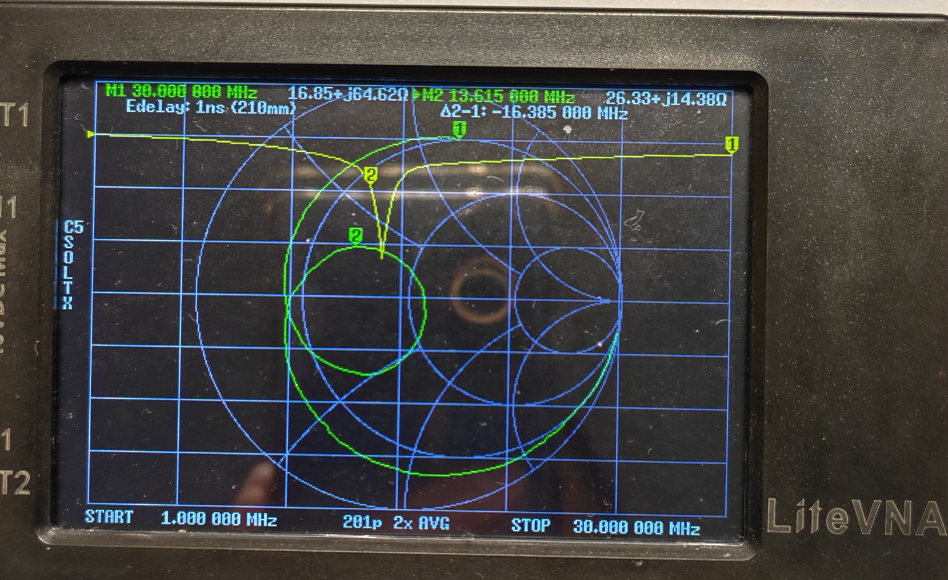
The Smith Chart can only be used to judge the adjustment trend; the actual values will differ from the simulation:
Actual component values: solder 220pF for C17 and C18 to move to the proper position on the VNA, and series 82pF to approach conjugate matching.
-
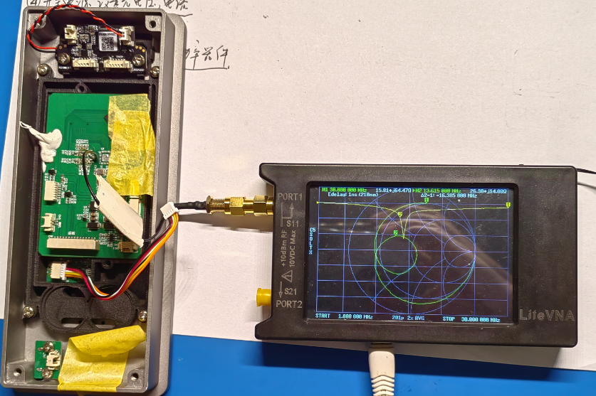
Verification test:
a. The reading distance has been adjusted to 1.5cm. Replace the series resistor R11 with 1Ω, and the distance increases to nearly 1.8cm.
b. After all values are adjusted, remove the two parallel 47Ω resistors and test the impedance of the entire link without the chip. The impedance of M2 is: Z=26.33+j14.38Ω, and S11 is also very good.
 About Maxipcb
Maxipcb empowers innovators to turn cutting-edge technologies into reality.
We offer one-stop solutions for design, simulation, testing, PCB manufacturing, component procurement and SMT assembly, enabling efficient development, rapid deployment and risk control across the full product lifecycle.Serving the world in communications, industrial automation, aerospace, automotive, semiconductor and beyond, we build a safer, more connected future together.


