There are many forms of noise in electronic systems. Whether it is received from external sources or transmitted between different areas of PCB layout, noise can be unintentionally received by two methods: parasitic capacitance and parasitic inductance. Parasitic inductance is relatively easy to understand and diagnose, both from the perspective of crosstalk and from the seemingly random noise coupling between different parts of the board.
There are many forms of noise in electronic systems. Whether it is received from external sources or transmitted between different areas of PCB layout, noise can be unintentionally received by two methods: parasitic capacitance and parasitic inductance. Parasitic inductance is relatively easy to understand and diagnose, both from the perspective of crosstalk and from the seemingly random noise coupling between different parts of the board.
Dealing with parasitic capacitance is not necessarily more difficult, but it does need to understand how PCB layout geometry will affect mutual capacitance. In high-frequency operating systems, or where high dV/dt nodes can create capacitive coupling noise, some simple PCB layout choices can help reduce parasitic components. In this paper, how to reduce parasitic capacitance will be generally described, and some examples in high frequency routing and switching converters will be provided.
Identify and reduce parasitic capacitance
Although there is no single formula for parasitic capacitance, it has a general definition:
Parasitic capacitance is an unintentional capacitance (usually undesirable) that exists between two conductive structures separated by an insulator.
Sometimes, this unexpected capacitance is actually beneficial. In this case, we don't use the word "parasitic" to describe it. Take the power-ground plane pair as an example; This simple structure helps to provide a large charge reserve to support high-speed components with high input/output number, because it is inherently capacitive. Another example is that in coplanar waveguide, parasitic capacitance is basically used to set the impedance of interconnection to a desired value.
In PCB, parasitic capacitance can appear almost anywhere. Look at the layout below; I pointed out some areas where parasitic capacitance is obvious. This only shows the capacitance generated by the top layer, but any layer may have capacitance.
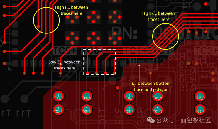
As the above definition implies, parasitic capacitance appears between any conductor pair separated by dielectric, and we can quickly identify multiple areas where parasitic capacitance appears in the above example. Whenever there is parasitic capacitance in PCB layout, it can appear in two ways:
As its own capacitance, it shows an undesirably high capacitance between a conductor and a different conductor (usually GND).
Mutual capacitance refers to the capacitance between two conductive structures, each of which refers to the third conductive structure; This is actually a capacitive form that leads to capacitive coupling between two traces.
Why is high parasitic capacitance important? This is important because whenever there is a changing potential between two capacitively coupled conductors, this will cause some displacement current to flow on each conductor. This is a form of crosstalk that designers should be familiar with. Usually, when a switching signal induces its signal on the victim trace, we call it crosstalk, but the same mechanism can also induce noise on any other structure when there are some parasitic capacitances.
Although it can never be completely eliminated, it is beneficial to try to reduce it in some cases. To understand some strategies to reduce parasitic capacitance, it is helpful to look at some examples.
Example: High dV/dt Node in Switching Regulator
The following regulator example section shows the location of a strong dV/dt node and why this layout has greater coupling into its feedback loop rather than to any nearby part of the system. In the switching regulator, the dV/dt node appears on the output of the switching stage, but before the rectification/filtering stage. In the following example, the SW_OUT node is our high dV/dt node, which is driven by PWM signal.
This node has some parasitic capacitance to the nearby ground area. If there are other components or circuits nearby, the parasitic capacitance of these circuits will cause switching noise to appear in these circuits. The nearby ground is helpful, but what really prevents noise coupling is the large capacitor returning from SW_OUT to the regulator chip. This large capacitor provides a low impedance path for high dV/dt switching noise to return to the high side of the switching stage, effectively decoupling the output of the switching stage from GND.
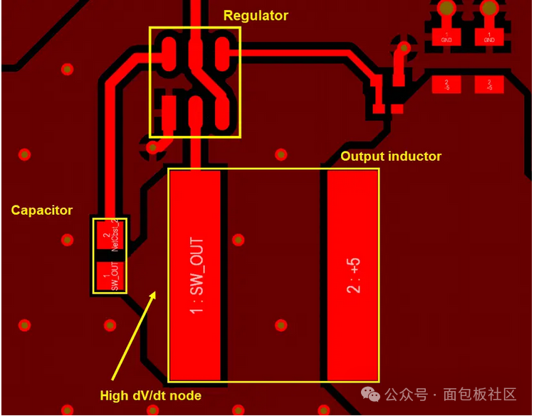
DV/dt nodes may cause noise coupling in PCB layout. A deliberately placed capacitor can prevent this.
Another strategy to reduce the parasitic capacitance between SW_OUT and nearby traces or circuits is to use the GND plane of the next layer. Placing the GND plane near the high dV/dt node will reduce the mutual capacitance compared with some other nodes in the PCB layout by creating a stronger coupling between the electric field and GND. In other words, it would be desirable to have a thinner dielectric layer between L1 and L2 of this board.
Example: Mutual capacitance between two traces
Capacitive crosstalk is one of the two coupling types between traces (the other is inductive), in which the signal on one trace can produce noise on the other. At increasing frequency, this is mainly dominated by mutual capacitance. In PCB layout, there are basically two options to reduce this type of parasitic capacitance, assuming that wiring has been done on GND area according to best practices:
-keeping the impedance target unchanged, make the ground wire closer to the signal line and make the signal line narrower at the same time.
-Increase the spacing between signal lines.
Almost all the suggestions you can find about reducing crosstalk will recommend option #2, but in fact option #1 is equally effective. This is because it brings the mirror charge/current in the ground plane closer to the signal line. Operations such as shorting the protection signal line should not be attempted, because this will generate undesirable parasitic capacitance on the ground line and actually increase crosstalk in some configurations.
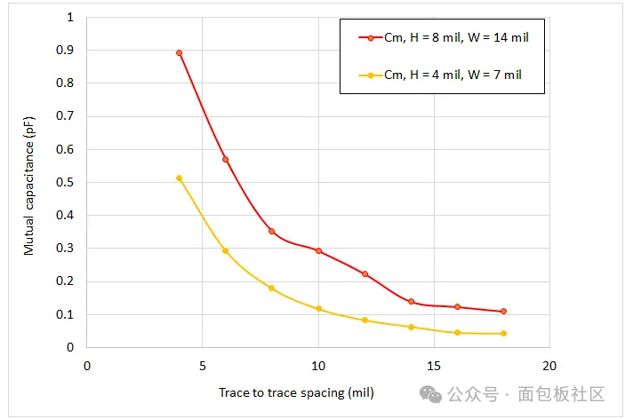
The simulation results show how the parasitic capacitance between two 50-ohm traces is affected by the distance (denoted as H) from the GND plane.
summary
For the parasitic capacitance in the form of self-capacitance, it is necessary to separate the conductors or make the conductors smaller. For the parasitic capacitance in the form of mutual capacitance, it is necessary to reduce the coupling by increasing the self capacitance far beyond the mutual capacitance. In the above example, we can see that their mutual capacitance is greatly reduced just by bringing the ground plane close to our mutual capacitance signal lines, without making any changes to other conductors in the PCB layout.
About Maxipcb
Maxipcb empowers innovators to turn cutting-edge technologies into reality.
We offer one-stop solutions for design, simulation, testing, PCB manufacturing, component procurement and SMT assembly, enabling efficient development, rapid deployment and risk control across the full product lifecycle.
Serving the world in communications, industrial automation, aerospace, automotive, semiconductor and beyond, we build a safer, more connected future together.


