With the continuous development of electronic technology, higher signal frequencies, steeper signal edges, smaller circuit board sizes, and higher routing densities in high-speed circuits have made signal integrity issues increasingly prominent in high-speed digital circuit design, which has become an unavoidable problem for high-speed circuit design engineers.
With the continuous development of electronic technology, higher signal frequencies, steeper signal edges, smaller circuit board sizes, and higher routing densities in high-speed circuits have made signal integrity issues increasingly prominent in high-speed digital circuit design, which has become an unavoidable problem for high-speed circuit design engineers.
Crosstalk refers to the transfer of unwanted signals from one network to another. It is an important issue in signal integrity and is ubiquitous in digital design, potentially occurring in devices such as chips, PCBs, connectors, chip packages, and connector cables.
If crosstalk exceeds a certain limit, it will cause false triggering of the circuit and lead to system malfunction. Therefore, it is very important for engineers to understand the mechanism of crosstalk and master the design methods to solve crosstalk.
01 Mechanism of Crosstalk Generation
Crosstalk is the unwanted voltage or current noise interference generated on adjacent transmission lines due to electromagnetic coupling when signals propagate on transmission lines. The fringe field effect of signal lines is the fundamental cause of crosstalk.
For ease of analysis, several related concepts are introduced below.
As shown in Figure 1, assuming the driver at point A is the interference source and the receiver at point D is the interfered object, the transmission line where driver A is located is called the aggressor network, and the corresponding transmission line network where receiver D is located is called the victim network.
Crosstalk on the victim network near the interference source is called near-end crosstalk (also known as backward crosstalk), while crosstalk far from the interference source is called far-end crosstalk (also known as forward crosstalk). According to different generation mechanisms, crosstalk can be divided into two categories: capacitive coupling crosstalk and inductive coupling crosstalk.
1.1 Capacitive Coupling Mechanism
When a signal is transmitted on the aggressor line, the change in signal edge voltage will induce a time-varying electric field in the area near the signal edge through the distributed capacitance on the aggressor line. Since the victim line is in this electric field, the changing electric field will generate an induced current on the victim line.
The signal edge can be regarded as a current source moving along the aggressor line, which continuously generates current noise on the victim line through capacitive coupling during its movement.
Since the impedance in each direction on the victim line is the same, 50% of the capacitive coupling current flows to the near end and the other 50% propagates to the far end.
In addition, the direction of capacitive coupling current is from the signal path to the return path, so the coupling currents propagating to the near end and the far end are both positive.
For near-end capacitive coupling crosstalk, as the driver outputs a rising edge pulse, the current flowing to the near end will increase rapidly from zero. When the edge has entered a saturation length, the near-end current will reach a fixed value.
In addition, the coupling current flowing to the near end will continuously flow to the near end at a constant speed. When the rising edge reaches the receiving end of the aggressor line, it will be absorbed by the receiver and no longer generate coupling current signals. However, there is still backward current flowing to the near end of the victim line, so the near-end coupling current will last for twice the transmission delay.
For far-end capacitive coupling crosstalk, since the signal edge can be regarded as a moving current source, it will generate coupling current flowing into the victim line through mutual capacitance in the area near the edge. The generated coupling current will have 50% flowing into the far end in the same direction and at the same speed as the signal on the aggressor line. Therefore, as the signal on the aggressor line propagates, forward coupling currents will be continuously generated on the victim line and superimposed with the existing forward coupling currents, propagating together to the far end.
Since crosstalk is only generated in the area near the signal edge, the duration of the coupling current flowing to the far end is equal to the signal transition time. The specific capacitive coupling is shown in Figure 2.
1.2 Inductive Coupling Mechanism
When a signal propagates on the aggressor line, the change in signal current will generate a time-varying magnetic field through the action of distributed inductance in the area near the signal transition. The changing magnetic field will induce a noise voltage on the victim line, thereby forming an inductive coupling current, which propagates to the near end and the far end respectively.
Unlike capacitive coupling current, the direction of inductive coupling current is opposite to the direction of signal propagation on the aggressor line. When propagating to the near end, the current loop is from the signal path to the return path, while when propagating to the far end, the current loop is from the return path to the signal path.
For near-end inductive coupling crosstalk, its characteristics are very similar to near-end capacitive coupling crosstalk. It also increases rapidly from zero, stabilizes at a fixed value when the transmission length is greater than or equal to the saturation length, and lasts for twice the transmission delay.
Since the inductive coupling current flowing to the near end is in the same direction as the capacitive coupling current, the two will be superimposed together.
For far-end inductive coupling crosstalk, the inductive coupling noise propagates at the same speed as the signal edge on the aggressor line, and more and more noise currents will be coupled at each step, with a duration equal to the signal transition time.
However, since the current direction is opposite to the far-end capacitive coupling current, the coupling current reaching the far-end receiver of the victim line is the difference between the two. The specific inductive coupling is shown in Figure 3.
1.3 Mixed Effect of Mutual Inductance and Mutual Capacitance
Generally, on a complete ground plane, the crosstalk voltages generated by capacitive and inductive coupling are equal in magnitude, so the total far-end crosstalk noise cancels each other out due to the opposite polarities of capacitive and inductive coupling.
Stripline circuits can better show the good balance between the two, with extremely small far-end coupling coefficients. However, for microstrip lines, since most of the electric field related to crosstalk passes through air rather than other insulating materials, capacitive crosstalk is smaller than inductive crosstalk, resulting in a small negative far-end crosstalk coefficient.
02 Simulation Analysis of Crosstalk
In actual design, board layer characteristics (such as thickness, dielectric constant, etc.), as well as line length, line width, line spacing, and signal rise time, all affect crosstalk.
The following analyzes the factors affecting crosstalk using Hyperlynx, a signal integrity simulation software from Mentor Graphics.
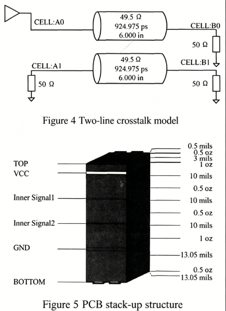
First, establish a two-wire crosstalk model in Hyperlynx, as shown in Figure 4. Set the line width of both lines to 5 mil, line length to 6 in, line spacing to 5 mil. Both lines are top-layer microstrip lines with a characteristic impedance of 49.5Ω. Both lines are terminated with 50Ω resistors to eliminate the effect of reflection.
The driver of the aggressor line adopts the IBIS model of CMOS process devices, with a voltage of 3.3V and a frequency of 100 MHz. The dielectric constant of the PCB is 4.3, and it is a 6-layer board with the stack-up structure shown in Figure 5.
2.1 Effect of Coupling Length on Crosstalk
Change the coupling length of the two lines to 3 in, 6 in, and 10 in respectively, keeping other settings unchanged.
Figure 6(a) shows the crosstalk waveform with a coupling length of 3 in, where the near-end crosstalk peak is 126.34 mV and the far-end is 43.01 mV; Figure 6(b) shows the crosstalk waveform with a coupling length of 6 in, with a near-end crosstalk peak of 153.23 mV and a far-end of 99.46 mV; Figure 6(c) shows the crosstalk waveform with a coupling length of 10 in, with a near-end crosstalk peak of 153.23 mV and a far-end of 163.98 mV.
It can be seen that the far-end crosstalk peak is proportional to the coupling length; the longer the coupling length, the greater the crosstalk. For near-end crosstalk, when the coupling length is less than the saturation length, crosstalk increases with the increase of coupling length, but when the coupling length is greater than the saturation length, the near-end crosstalk value will be a stable value.
2.2 Effect of Line Spacing on Crosstalk
The following examines the effect of changes in line spacing on crosstalk while keeping other settings unchanged. Set the line spacing to 5 mil and 15 mil respectively, and the simulation waveforms are shown in Figure 7.
It can be seen from Figure 7 that when the line spacing is 5 mil, the near-end crosstalk peak is 153.23 mV and the far-end is 99.46 mV; when the line spacing is 15 mil, the near-end crosstalk peak is 33.40 mV and the far-end is 40.49 mV.
It can be seen that as the line spacing increases, both near-end and far-end crosstalk decrease. When the line spacing is greater than or equal to 3 times the line width, crosstalk is already very small.
2.3 Effect of Rise Time on Crosstalk
The following examines the effect of changes in rising edge time on crosstalk, keeping other settings unchanged. Set the drivers to CMOS 3.3V MEDIUM, CMOS 3.3V FAST, and CMOS 3.3V ULTRA-FAST respectively, and the simulation waveforms are shown in Figure 8.
In Figure 8(a), the near-end crosstalk peak is 153.9 mV and the far-end crosstalk is 46.3 mV; in Figure 8(b), the near-end crosstalk peak is 153.2 mV and the far-end crosstalk is 99.5 mV; in Figure 8(c), the near-end crosstalk peak is 153.2 mV and the far-end crosstalk is 349.9 mV.
It can be seen that as the rising edge time shortens, the far-end crosstalk noise becomes larger and larger.
For near-end crosstalk, if the rise time is shorter compared to the transmission line delay, near-end crosstalk is independent of the rise time; if the rise time is longer compared to the transmission line delay, the near-end crosstalk noise is related to the rise time (near-end crosstalk increases as the rising edge time decreases).
2.4 Effect of Dielectric Layer Thickness on Crosstalk
Set the dielectric layer thickness to 3 mil and 6 mil respectively in the PCB stack-up editor, keeping other settings unchanged. The simulation waveforms are shown in Figure 9.
Examining the above simulation waveforms, it can be seen that when the dielectric layer thickness is 3 mil, the near-end crosstalk peak is 153.2 mV and the far-end crosstalk is 99.5 mV; when the dielectric layer thickness is 6 mil, the near-end crosstalk peak is 277.3 mV and the far-end crosstalk is 163.9 mV.
It can be seen that as the dielectric layer thickness decreases, crosstalk also decreases.
03 Methods to Solve Crosstalk
Crosstalk is ubiquitous in the design of electronic products. Through the above analysis and simulation, we have understood the characteristics of crosstalk and summarized the following methods to reduce crosstalk:
(1) When conditions permit, increase the distance between traces as much as possible, reduce the length of parallel traces, and adopt jog routing if necessary.
(2) While ensuring signal timing, select devices with slower rising and falling edge speeds as much as possible to slow down the change speed of electric and magnetic fields, thereby reducing crosstalk.
(3) When designing traces, conductors should be as close as possible to the ground plane or power plane. This allows the signal path to be tightly coupled with the ground plane, reducing interference to adjacent signal lines.
(4) If routing space permits, insert a ground line between two signal lines with severe crosstalk to reduce the coupling between the two signal lines and thus reduce crosstalk.
04 Conclusion
Crosstalk is an important part of signal integrity, which affects the timing of the system, reduces the noise margin, and leads to system malfunction.
This article introduces the mechanism of crosstalk generation in high-speed circuits, analyzes crosstalk through simulation, obtains the relationship between the magnitude of crosstalk and related factors affecting crosstalk, and proposes some methods to reduce crosstalk on this basis, which has certain guiding significance for solving crosstalk problems in high-speed and high-density circuit design.
About Maxipcb
Maxipcb enables advanced electronic innovation. We deliver one-stop solutions including circuit design, simulation, testing, PCB fabrication, component sourcing and SMT&PCBA assembly, to boost R&D efficiency, speed up mass production and control full-cycle risks. We serve global sectors like communication, industrial automation, aerospace, automotive and semiconductor, jointly forging a safer, connected intelligent future.


