Component layout on a PCB is of paramount importance. A correct and reasonable layout not only makes the board neat and aesthetically pleasing but also affects the length and number of printed conductors. A well-designed PCB component layout is extremely significant for improving the overall performance of the equipment.
Component layout on a PCB is of paramount importance. A correct and reasonable layout not only makes the board neat and aesthetically pleasing but also affects the length and number of printed conductors. A well-designed PCB component layout is extremely significant for improving the overall performance of the equipment.
So how to achieve a more reasonable layout? Today, we will share several key details of PCB layout.
01 Key Layout Points for PCBs with Wireless Modules
- Physically separate analog circuits from digital circuits; for example, keep the antenna ports of MCUs and wireless modules as far apart as possible.
- Avoid routing high-frequency digital traces, high-frequency analog traces, power traces, and placing other sensitive components under wireless modules as much as possible; copper pouring can be performed under the modules.
- Keep wireless modules as far away as possible from components with strong electromagnetic interference such as transformers, high-power inductors, and power supplies.
- When placing on-board PCB antennas or ceramic antennas, the PCB under the antenna part of the module shall be hollowed out without copper pouring, and the antenna part shall be located at the edge of the board as much as possible.
- Both RF signals and other signal traces shall be as short as possible; other signals shall also be kept away from the transmitting part of the wireless module to avoid interference.
- The layout shall ensure that the wireless module has a complete power and ground plane, and RF traces shall reserve space for accompanying ground vias.
- Wireless modules have high requirements for voltage ripple, so it is best to add appropriate filter capacitors close to the voltage pins of the module, such as 10μF capacitors.
- Wireless modules have fast transmission frequencies and certain requirements for power supply transient response. In addition to selecting excellent power supply solutions during design, the power supply circuits shall be reasonably arranged during layout to fully exert the power supply performance; for example, in DC-DC layout, the distance between the ground of the freewheeling diode and the IC ground shall be as close as possible to ensure return current, and the distance between the power inductor and the capacitor shall be as close as possible.
02 Setting of Trace Width and Trace Spacing
The setting of trace width and trace spacing has a huge impact on the performance improvement of the entire board. Reasonable settings of trace width and spacing can effectively improve the electromagnetic compatibility and various performances of the board.
For example, the setting of power trace width shall consider the load current, supply voltage, PCB copper thickness, trace length and other factors. Generally, a trace with a width of 1.0mm and a copper thickness of 1oz (0.035mm) can carry approximately 2A of current. Reasonable setting of trace spacing can effectively reduce crosstalk and other phenomena, such as the commonly used 3W rule (when the center-to-center spacing between conductors is not less than 3 times the trace width, 70% of the electric field can be kept from interfering with each other).
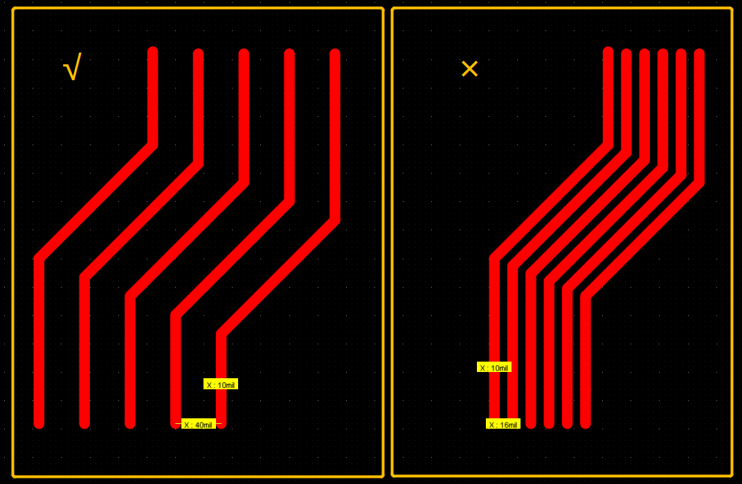
- Power traces: Comprehensively considered according to load current, voltage and PCB copper thickness. Generally, the current shall be reserved with 2 times the normal operating current, and the trace spacing shall meet the 3W rule as much as possible.
- Signal traces: Comprehensively considered according to signal transmission rate, transmission type (analog or digital), trace length, etc. The spacing of ordinary signal lines is recommended to meet the 3W rule, and differential lines shall be considered separately.
- RF traces: The line width of RF traces shall consider the characteristic impedance. The antenna interfaces of commonly used RF modules all have a characteristic impedance of 50Ω. According to experience, the RF line width is 0.55mm and the copper pouring spacing is 0.5mm for power ≤30dBm (1W). More accurate characteristic impedance of approximately 50Ω can also be obtained with the assistance of the board manufacturer.
03 Setting of Spacing Between Components
The spacing between components is a must-consider issue in PCB Layout. If the spacing is too small, it is easy to cause solder bridging during soldering and affect production.
The recommended distances are as follows:
- Similar components: ≥0.3mm
- Different components: ≥0.13*h + 0.3mm (h is the maximum height difference of adjacent surrounding components)
- Recommended distance between components that can only be soldered manually: ≥1.5mm
- Through-hole components and surface-mount components shall also maintain sufficient production distance, recommended between 1-3mm.
04 Spacing Control Between Board Edge and Components/Traces
The rationality of the distance design between components/traces and the board edge during PCB layout and routing is also very important. For example, panelization is mostly used in the actual production process. Therefore, if components are too close to the board edge, it will cause pad peeling or even component damage during PCB depaneling; if traces are too close, it is easy to cause trace breakage during production and affect circuit functions.
Recommended Distances and Placement Methods
- Component placement: It is recommended that the component pads be parallel to the "V-cut" direction of the panel. The purpose is to make the mechanical stress on the component pads uniform and the force direction the same during depaneling, reducing the possibility of pad peeling.
- Component distance: The placement distance of components from the board edge ≥0.5mm
- Trace distance: The distance of traces from the board edge ≥0.5mm
05 Adjacent Pad Connection and Teardrops
If adjacent pins of an IC need to be connected, it is best not to connect directly on the pads, but to lead out and connect outside the pads. This can prevent solder bridging and short circuit of IC pins during production. In addition, attention shall be paid to the line width of the leads between adjacent pads, which should preferably not exceed the size of the IC pins, except for some special pins such as power pins.
Teardrops can effectively reduce reflection caused by sudden changes in line width, allowing smooth connection between traces and pads;
Adding teardrops solves the problem that the connection between traces and pads is easily broken by impact force;
In terms of appearance, adding teardrops also makes the PCB look more reasonable and beautiful.
06 Parameters and Placement of Vias
The rationality of via size setting has a great impact on circuit performance. Reasonable via size setting needs to consider the current carried by the via, signal frequency, manufacturing process difficulty and other factors, so special attention shall be paid to PCB Layout.
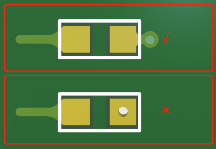
In addition, the placement of vias is equally important. If vias are placed on pads, it is easy to cause poor soldering of components during production. Therefore, vias are generally placed outside the pads. Of course, in extremely tight space conditions, placing vias on pads combined with the via-in-pad process of the board manufacturer is also feasible, but this will increase production costs.
Key Points for Via Setting
- Different sizes of vias can be placed in a PCB according to the needs of different traces, but it is generally not recommended to exceed 3 types to avoid great inconvenience to production and increase costs.
- The ratio of via depth to diameter is generally ≤6, because when it exceeds 6 times, it is difficult to ensure uniform copper plating on the hole wall during production.
- Attention shall also be paid to the parasitic inductance and parasitic capacitance of vias, especially their distribution performance parameters in high-speed circuits.
- Smaller vias have smaller distribution parameters and are more suitable for high-speed circuits, but their cost is also higher.
The above 6 points are some precautions for PCB Layout sorted out this time, hoping to be helpful to everyone.
About Maxipcb
Maxipcb enables advanced electronic innovation. We deliver one-stop solutions including circuit design, simulation, testing, PCB fabrication, component sourcing and SMT&PCBA assembly, to boost R&D efficiency, speed up mass production and control full-cycle risks. We serve global sectors like communication, industrial automation, aerospace, automotive and semiconductor, jointly forging a safer, connected intelligent future.


