In the field of PCB design, "impedance" is the key to determine whether the signal can be transmitted stably. Many engineers have ignored impedance matching and encountered problems such as signal reflection and crosstalk, which led to repeated jamming in product debugging. In fact, as long as you master the core logic of impedance calculation, you can easily deal with it from parameter preparation to software operation.
In the field of PCB design, "impedance" is the key to determine whether the signal can be transmitted stably. Many engineers have ignored impedance matching and encountered problems such as signal reflection and crosstalk, which led to repeated jamming in product debugging. In fact, as long as you master the core logic of impedance calculation, you can easily deal with it from parameter preparation to software operation. In today's article, the whole process of impedance calculation is disassembled in popular language, with detailed cases, and novices can get started quickly!
First, why must I do impedance calculation?
The root of the signal "can't run" is hereWhen the voltage and current propagate in the transmission line, if the characteristic impedance is inconsistent, it will appear "signal reflection" just like the sound hitting the wall to produce echo. In the field of signal integrity, common problems such as reflection, crosstalk and power plane cutting are all caused by "impedance discontinuity" in essence.
Especially for high-frequency and high-speed PCB design, impedance mismatch will directly affect the signal transmission speed and stability, and even lead to product function failure. Therefore, impedance matching through accurate calculation is the core step to ensure the performance of PCB, which is indispensable!
Two. three kinds of core impedance models,
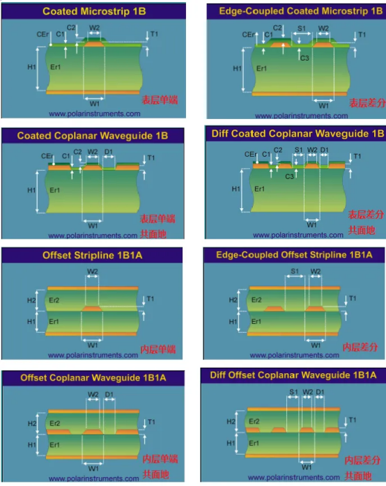
one picture distinguishes the difference between inner layer and outer layer.Before impedance calculation, we must first make clear what model to use. Commonly used Polar.SI9000 tools are mainly developed around three types of impedance models, and each type of model is subdivided into inner and outer versions, which are classified as follows:
Characteristic impedance model: outer layer characteristic impedance model and inner layer characteristic impedance model.
Differential impedance model: outer differential impedance model and inner differential impedance model.
Coplanarity impedance model: outer coplanar characteristic impedance, inner coplanar characteristic impedance, outer coplanar differential impedance and inner coplanar differential impedance.
The structural differences of various models can be intuitively understood with reference to the following figure:
Third, you must understand before calculation:
7 necessary conditions+6 influencing factorsImpedance calculation is not "just filling in numbers". It is necessary to make clear the core parameters first and then clarify the influencing factors to ensure the accuracy of the results.
1. Seven prerequisites: one less is not enough.
Just like cooking needs ingredients, impedance calculation must prepare the following seven parameters in advance:
Thickness: overall thickness of PCB.
Layers: including signal layers and power layers.
Plate: such as FR-4, Rogers, etc.
Surface technology: gold plating, tin spraying, etc.
Impedance value: design target (such as 50Ω, 90Ω).
Impedance tolerance: allowable error range (such as 10%)
Copper thickness: thickness of inner and outer copper foil (1OZ=0.035mm, commonly used unit).
2. Six key influencing factors: parameter meaning Look at this picture.
The impedance value will be affected by six factors, and the specific definition of each factor can be understood by the parameter annotation in the figure below:
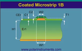
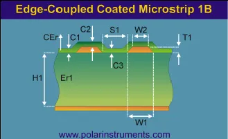
The specific meanings of each parameter are as follows:
H1: dielectric thickness (PP sheet or plate, excluding copper thickness)
Er1: Dielectric constant (average value when pressing various PP/plates)
W1: line width of impedance line; W2: line width on impedance line
T1: finished copper thickness
Cer: dielectric constant of green oil (fixed value 3.3)
C1: green oil thickness of substrate (usually calculated by 0.8mil)
C2: thickness of green oil on copper skin/wiring (usually calculated as 0.5mil)
Zo: the final calculated theoretical impedance value.
3. Tip: Upper and Lower Line Width Relation Table
The upper and lower line widths (W1 and W2) are not fixed values, and will be affected by the copper thickness and process. Please refer to the following table for the specific corresponding relationship, and look it up directly when calculating:
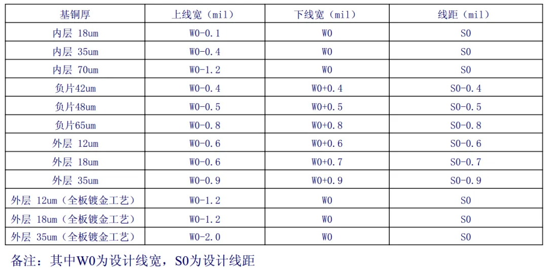
(Note: in the table, W0 is the design line width, S0 is the design line spacing, and different copper thicknesses and processes correspond to different offset values.)
Fourth, quick check of plate parameters: FR-4, Rogers does not need to turn over the manual.
Dielectric constant and thickness of plates are the core inputs of impedance calculation, and the parameters of different plates are quite different. Here, the key data of commonly used plates are sorted out and applied directly.
1. Common FR-4 core board: Shengyi and equivalent materials.
FR-4 is the most commonly used plate. The corresponding relationship between the thickness (mm/mil) and dielectric constant of FR-4 core plate is as follows, and it should be selected according to the thickness requirement in design:

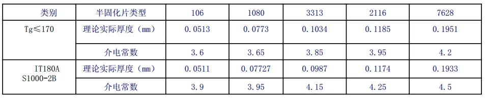
2. PP sheet (prepreg): common model parameters are fixed.
PP sheet is the key material for lamination. The thickness and dielectric constant of common models are as follows:
Type 106: thickness 0.04mm
Type 1080: thickness 0.06mm
Type 2116: thickness 0.11 mm.
Type 7628: thickness 0.19mm
Refer to the following table for specific parameters:
3. Rogers sheet: a must for high-frequency design
Rogers plate is commonly used in high-frequency PCB, and its dielectric constant is stable. The key parameters are as follows:
Rogers4350:0.1mm mm thickness has a dielectric constant of 3.36, and other thicknesses are 3.48.
Rogers4003: Dielectric constant 3.38
Rogers4403 prepreg: dielectric constant 3.17
4. Precautions for lamination: Avoid "stepping on the pit"
Multilayer board is made of core board and PP sheet by pressing, and four rules should be observed to avoid the problems of interlayer dislocation and poor appearance:
4 or more PP sheets are not allowed to be stacked, which is easy to "slide" (interlayer dislocation)
7628 PP sheet can not be put on the outer layer, and the rough surface affects the appearance.
Three 1080 PP sheets can't be put on the outer layer, which is also easy to slide.
CORE thickness ≥0.11mm, 2 cores for 6-layer board and 3 cores for 8-layer board.
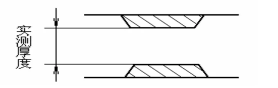
V. Measured thickness ≠ Theoretical thickness!
This formula helps you calibrate.When calculating, it will be found that there is a deviation between the theoretical plate thickness and the actual measured value, and the problem lies in the "copper thickness" and "copper residue rate"
1. Residual copper rate: how to define it? How to get the value?
The residual copper rate is the ratio of "the area with copper on the board/the whole board area":
Raw materials: 100%
Etched optical plate: 0%
Power ground plane: usually 70%
Signal layer: usually 23%
Surface layer: take 1 (default full copper coverage)
2. Calculation formula of measured thickness
To get the accurate measured thickness, use the following formula to calculate: measured thickness = theoretical thickness-copper thickness 1×(1-X1)- copper thickness 2×(1-X2)(X1 and X2 are the residual copper rate of the corresponding layer, and the unit of copper thickness is 1OZ=0.035mm).
The difference between the theoretical thickness and the measured thickness can be understood with reference to the following figure:
 Sixth, the actual combat case:
the whole process of impedance calculation of 6-layer boardJust talk and don't practice the trick. Here, taking a 6-layer board as an example, we will take you through the impedance calculation steps from demand analysis to result output.
1. Clear design requirements (known conditions)
Thickness: 1.2mm (allowable error ±0.12mm)
Plate: FR-4
Number of floors: 6 floors
Copper thickness: 1OZ for inner layer and 0.5OZ for surface layer.
Target impedance: 50Ω single-line impedance in the surface layer and 90Ω differential impedance in the inner layer.
2. Design laminated structure
According to the parameters of core board and PP sheet, combined with the thickness requirements, the 6-layer laminated structure is designed as follows, and the key parameters have been marked:
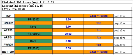
Key calculation: measured thickness of PP sheet
Measured value of PP(3313) = 0.1034mm (theoretical value) -0.035/2mm×(1-1) (surface layer 0.5OZ, copper residual rate 1)-0.035mm×(1-0.7) (inner layer 1OZ, copper residual rate 70%) = 0.0929 mm = 3.
The measured value of PP(7628*3) = 0.1951×3mm (theoretical value) -0.035×(1-0.23) (1OZ in inner layer, 23% in signal layer) × 2 = 0.5314 mm = 20.92 mil.
Total thickness verification
Total thickness of board
= 0.5oz+3.65mil+1oz+5.1mil+1oz+20.92mil+1oz+5.1mil+1oz+3.65mil+0.5oz = 1.15mm, which meets the requirement of 1.2±0.12mm.
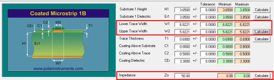
3. Calculation of surface 50Ω single-line impedance (SI9000 practical operation)
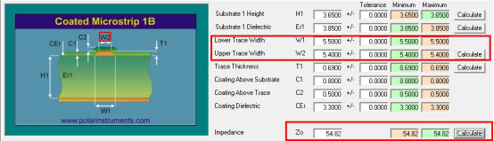
Open SI9000 software, select "external layer characteristic impedance model", fill in lamination parameters (H1=3.65mil, Er1=3.85, T1=0.69mil, etc.), and calculate the theoretical line width W0=6.8mil.
Considering the actual wiring difficulty, the line width can be fine-tuned: when the line width is adjusted to 5.5mil, the impedance Zo=54.82Ω, within the tolerance range of 50 Ω 10% (45-55 Ω), which meets the requirements.
Computing interface reference
5. Summary of final calculation results
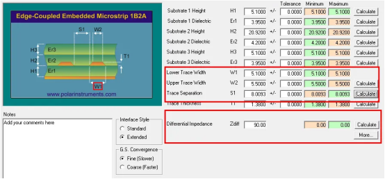
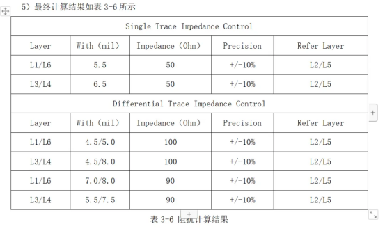
All impedance calculation results are arranged as follows, which can be used for direct reference in design:
 summary:
Impedance calculation seems complicated, but in fact it is a standardized process of "parameter preparation → model selection → software calculation → fine tuning of results". As long as you master the meaning of necessary parameters, sheet characteristics and lamination rules, and practice with actual cases, you can easily get it. I hope this article can help you avoid the "pit" of signal integrity and make PCB design more efficient!
About Maxipcb
Maxipcb empowers innovators to turn cutting-edge technologies into reality.
We offer one-stop solutions for design, simulation, testing, PCB manufacturing, component procurement and SMT assembly, enabling efficient development, rapid deployment and risk control across the full product lifecycle.
Serving the world in communications, industrial automation, aerospace, automotive, semiconductor and beyond, we build a safer, more connected future together.

