A well-laid-out PCB eliminates ESD troubles. To improve electrostatic discharge (ESD) protection, the following points must be implemented in PCB design:
A well-laid-out PCB eliminates ESD troubles. To improve electrostatic discharge (ESD) protection, the following points must be implemented in PCB design:
For the rectification of power supply layout, refer to
Figure 1.
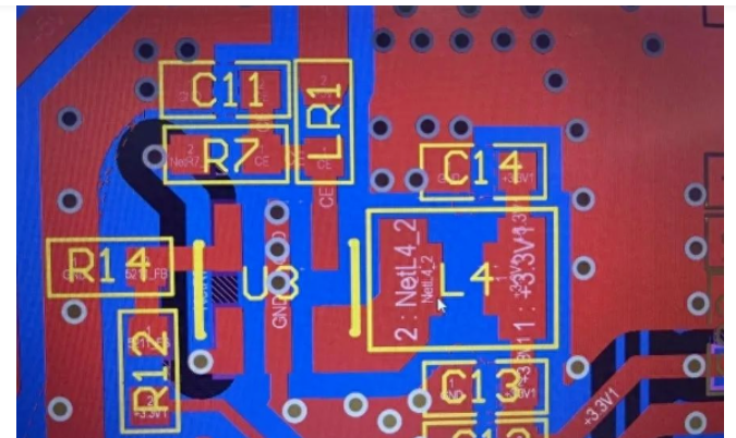
- DCDC Power Supply Layout: At the voltage output terminal, the inductor, bypass capacitors, and energy storage capacitors shall be arranged as shown in the figure. Bypass capacitors C14 and C13 should be placed as close to the inductor output as possible, and voltage sampling should be performed after capacitor C12. This aims to achieve better filtering and reduce interference in the circuit.
- High-Frequency Bypass Capacitors: All high-frequency bypass capacitors on power lines and signal lines should be grounded as close as possible to reduce the large ESD current entering the circuit system and achieve better interference absorption.
- Reset and Factory-Reset Signal Lines: Keep reset lines and factory-restore signal lines as short as possible, since longer traces are less resistant to ESD energy. Therefore, components should be placed close to each other to shorten trace lengths. If unavoidable, the traces should be surrounded by ground on both sides, as shown in Figure 2.
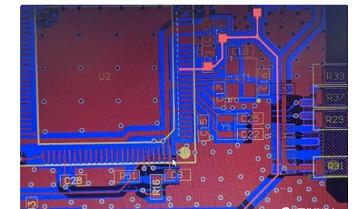 This reduces interference from other signals and prevents unexpected chip resets. Additionally, capacitors or resistors can be added to the circuit to increase internal resistance and block excessive interference signals.
- Switch Reset Line Layout: Follow the same principle for switch reset line layout. A π-type filter circuit can be added to the circuit, as shown in Figure 3, to better eliminate external interference and prevent chip reset.
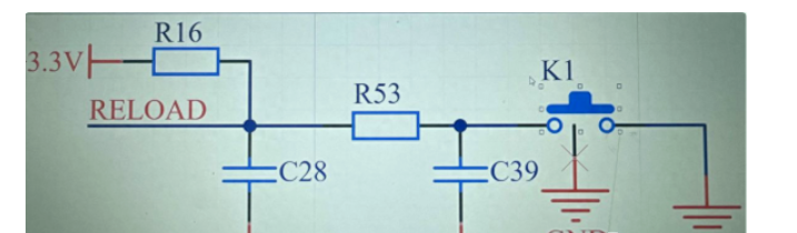
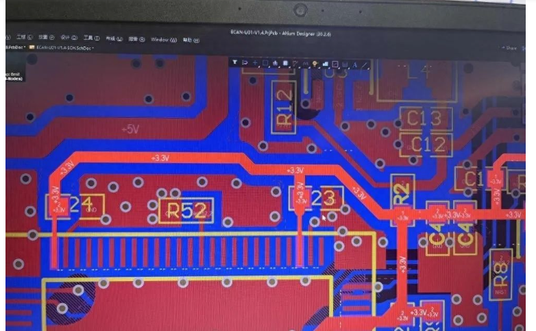
- Chip Power Supply Routing: For chip power supply, power traces should pass through capacitors before reaching the chip to provide protection, as shown in Figure 4.
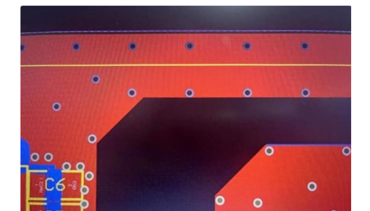
- Ground Copper Pouring: Avoid right-angle corners in ground copper pouring; use corners greater than 90°. Right-angle tips generate interference and cause inconsistent discharge paths, as shown in Figure 5.
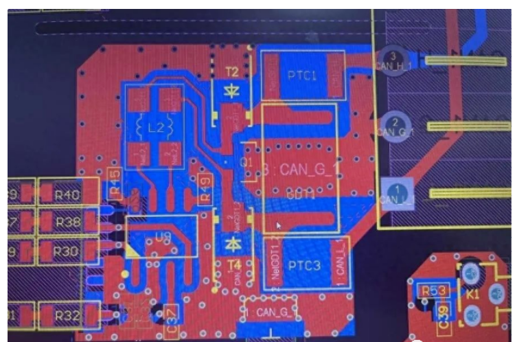
- Communication Line Protection: Communication lines should first pass through protection devices, then through surge arresters for discharge (surge arresters grounded nearby), and finally through TVS diodes for discharge. Keep traces as short as possible and loops as small as possible to quickly eliminate interference signals. Y-capacitors added to the ground line enable fast discharge and ESD elimination, as shown in Figure 6.
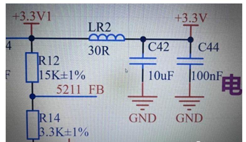
- Separate Power Supply for Chips: Power the MCU and other chips separately to avoid mutual interference, and add LC filter circuits to the circuit as shown in Figure 7.
- Multilayer PCB Application: Use multilayer PCBs, which greatly improve the system’s resistance to ESD discharge. Place the first-layer ground plane as close to the signal routing layer as possible to quickly cancel ESD transient discharge when it reaches the traces.
- Electrical Isolation: Electrical isolation is another method to suppress ESD surge impacts. Add isolation chips, optocouplers, transformers, etc., on the PCB. Combining cut-off isolation and shielding effectively suppresses ESD surge impacts.
In summary, the layout of the power plane, ground plane, and signal lines is one of the key measures for PCB ESD protection design to prevent ESD interference.
About Maxipcb
Maxipcb empowers innovators to turn cutting-edge technologies into reality.
We offer one-stop solutions for design, simulation, testing, PCB manufacturing, component procurement and SMT assembly, enabling efficient development, rapid deployment and risk control across the full product lifecycle.Serving the world in communications, industrial automation, aerospace, automotive, semiconductor and beyond, we build a safer, more connected future together.

 This reduces interference from other signals and prevents unexpected chip resets. Additionally, capacitors or resistors can be added to the circuit to increase internal resistance and block excessive interference signals.
