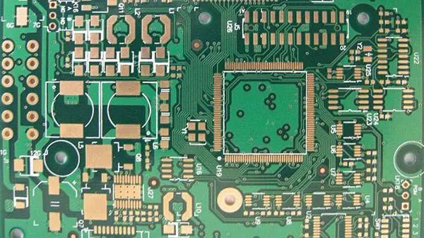
Vias are one of the important components of multi-layer PCBs, and drilling costs usually account for 30% to 40% of PCB manufacturing costs. Simply put, every hole on a PCB can be called a via.
Vias are one of the important components of multi-layer PCBs, and drilling costs usually account for 30% to 40% of PCB manufacturing costs. Simply put, every hole on a PCB can be called a via.
Basic Concepts of Vias
In terms of function, vias can be divided into two categories: one is used for electrical connection between layers, and the other is used for fixing or positioning components. In terms of manufacturing process, these vias are generally divided into three types: blind vias, buried vias, and through-hole vias.
Blind vias are located on the top and bottom surfaces of printed circuit boards with a certain depth, used to connect surface circuits to the underlying inner circuits. The depth of the holes usually does not exceed a certain ratio (to the hole diameter).
Buried vias are connection holes located in the inner layers of printed circuit boards, which do not extend to the surface of the board. Both of the above two types of vias are located in the inner layers of the board and are completed using the through-hole forming process before lamination. Several inner layers may be overlapped during the via formation process.
The third type is called through-hole vias, which pass through the entire circuit board and can be used for internal interconnection or as mounting and positioning holes for components. Since through-hole vias are easier to implement in terms of technology and have lower costs, the vast majority of printed circuit boards use them instead of the other two types of vias. Unless otherwise specified, the vias mentioned below refer to through-hole vias.
From a design perspective, a via mainly consists of two parts: the central drill hole and the pad area around the drill hole. The sizes of these two parts determine the size of the via.
Obviously, in high-speed and high-density PCB design, designers always hope that vias are as small as possible, so that more routing space can be left on the board. In addition, smaller vias have smaller parasitic capacitance, making them more suitable for high-speed circuits.
However, the reduction in hole size also brings an increase in cost, and the size of vias cannot be reduced indefinitely. It is limited by drilling and electroplating technologies: the smaller the hole, the longer the drilling time and the easier it is to deviate from the center position; and when the depth of the hole exceeds 6 times the drilling diameter, it is impossible to ensure uniform copper plating on the hole wall.
For example, if the thickness (through-hole depth) of a normal 6-layer PCB is 50 mils, the minimum drilling diameter that PCB manufacturers can provide under general conditions is only 8 mils. With the development of laser drilling technology, the size of drill holes can also become smaller and smaller. Generally, vias with a diameter of 6 mils or less are called microvias.
Microvias are often used in HDI (High-Density Interconnect) design. Microvia technology allows vias to be drilled directly on pads, which greatly improves circuit performance and saves routing space. Vias appear as discontinuous impedance breakpoints on transmission lines, causing signal reflection.
Generally, the equivalent impedance of a via is about 12% lower than that of the transmission line. For example, a 50-ohm transmission line will have an impedance reduction of 6 ohms when passing through a via (the specific value is related to the via size and board thickness, not an absolute reduction).
However, the reflection caused by impedance discontinuity of vias is actually negligible, with a reflection coefficient of only:
(44-50)/(44+50)=0.06
The problems caused by vias are more concentrated in the effects of parasitic capacitance and inductance.
Parasitic Capacitance and Inductance of Vias
Vias themselves have parasitic stray capacitance. If the diameter of the solder mask area of the via on the ground plane is D2, the diameter of the via pad is D1, the thickness of the PCB is T, and the dielectric constant of the board substrate is ε, then the parasitic capacitance of the via is approximately:
C=1.41εTD1/(D2-D1)
The main effect of the parasitic capacitance of vias on the circuit is to prolong the signal rise time and reduce the circuit speed.
For example, for a PCB with a thickness of 50 mils, if the via pad diameter used is 20 mils (drill diameter 10 mils) and the solder mask area diameter is 40 mils, we can approximately calculate the parasitic capacitance of the through the above formula:
C=1.41×4.4×0.050×0.020/(0.040-0.020)=0.31pF
The rise time change caused by this part of the capacitance is approximately:
T10-90=2.2C(Z0/2)=2.2×0.31×(50/2)=17.05ps
It can be seen from these values that although the effect of the parasitic capacitance of a single via on slowing down the rising edge is not obvious, if multiple vias are used for layer switching in the routing, multiple vias will be involved, and careful consideration should be taken during design. In actual design, parasitic capacitance can be reduced by increasing the distance between the via and the copper pouring area (Anti-pad) or reducing the pad diameter.
While vias have parasitic capacitance, they also have parasitic inductance. In the design of high-speed digital circuits, the harm caused by the parasitic inductance of vias is often greater than the effect of parasitic capacitance. Its parasitic series inductance weakens the contribution of bypass capacitors and reduces the filtering effectiveness of the entire power supply system.
We can use the following empirical formula to simply calculate the approximate parasitic inductance of a via:
L=5.08h[ln(4h/d)+1]
Where L is the inductance of the via, h is the length of the via, and d is the diameter of the central drill hole. It can be seen from the formula that the diameter of the via has a small effect on the inductance, and the length of the via has the greatest effect on the inductance. Still using the above example, the inductance of the via can be calculated as:
L=5.08×0.050[ln(4×0.050/0.010)+1]=1.015nH
If the signal rise time is 1ns, its equivalent impedance is:
XL=πL/T10-90=3.19Ω
Such impedance cannot be ignored when high-frequency currents pass through. Special attention should be paid that bypass capacitors need to pass through two vias when connecting the power layer and the ground layer, so the parasitic inductance of the vias will double.
How to Use Vias
Through the above analysis of the parasitic characteristics of vias, we can see that in high-speed PCB design, seemingly simple vias often bring great negative effects to circuit design. To reduce the adverse effects caused by the parasitic effects of vias, the following can be done as much as possible in the design:
- Select a reasonable via size considering both cost and signal quality. If necessary, consider using different sizes of vias. For example, larger vias can be used for power or ground lines to reduce impedance, while smaller vias can be used for signal traces. Of course, as the via size decreases, the corresponding cost increases.
- It can be concluded from the two formulas discussed above that using thinner PCBs helps reduce both parasitic parameters of vias.
- Signal traces on the PCB should avoid layer switching as much as possible, that is, try not to use unnecessary vias.
- Vias should be drilled as close as possible to the pins of power and ground, and the leads between vias and pins should be as short as possible. Consider drilling multiple vias in parallel to reduce equivalent inductance.
- Place some ground vias near the vias where signals switch layers to provide the nearest return path for signals. Even some redundant ground vias can be placed on the PCB.
- For high-density high-speed PCBs, consider using microvias.
About MaxipcbMaxipcb enables advanced electronic innovation. We deliver one-stop solutions including circuit design, simulation, testing, PCB fabrication, component sourcing and SMT&PCBA assembly, to boost R&D efficiency, speed up mass production and control full-cycle risks. We serve global sectors like communication, industrial automation, aerospace, automotive and semiconductor, jointly forging a safer, connected intelligent future.


