29 Fundamental Relationships Between Layout and PCB
- Several basic principles: Any conductor has impedance; current always automatically selects the path with the lowest impedance; radiation intensity is related to current, frequency, and loop area; common-mode interference is related to the mutual capacitance of large dv/dt signals to ground; the principles of reducing EMI and enhancing anti-interference capability are similar.
- Layout should be partitioned according to power supply, analog, high-speed digital, and various functional blocks.
- Minimize the area of large di/dt loops, reduce the length (or area, the width should not be too wide; increased routing area increases distributed capacitance, the general practice is: make the trace width as large as possible but remove redundant parts) of large dv/dt signal lines, and route them as straight as possible to reduce their implicitly enclosed area and thus reduce radiation.
- Inductive crosstalk is mainly caused by large di/dt loops (loop antennas), and the induction intensity is proportional to mutual inductance. Therefore, reducing mutual inductance with these signals (main approaches: reducing loop area, increasing distance) is critical; capacitive crosstalk is mainly generated by large dv/dt signals, and the induction intensity is proportional to mutual capacitance. Therefore, reducing mutual capacitance with these signals (main approaches: reducing effective coupling area, increasing distance; mutual capacitance decreases rapidly with increasing distance) is critical.
- Route wires using the loop cancellation principle as much as possible to further reduce the area of large di/dt loops, as shown in Figure 1 (similar to twisted pairs using the loop cancellation principle to improve anti-interference capability and increase transmission distance):
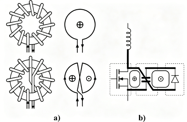
- Reducing loop area not only reduces radiation but also reduces loop inductance, resulting in better circuit performance.
- Reducing loop area requires us to accurately design the return path of each trace.
- When multiple PCBs are connected through connectors, it is also necessary to minimize the loop area, especially for large di/dt signals, high-frequency signals, or sensitive signals. Preferably, one signal line corresponds to one ground line, and the two lines should be as close as possible. Twisted pairs can be used for connection if necessary (the length of each turn of the twisted pair corresponds to an integer multiple of the half-wavelength of the noise). If you open a computer case, you can see that the connection from the motherboard to the front panel USB interface uses twisted pairs, which shows the importance of twisted pair connections for anti-interference and radiation reduction.
- For data cables, arrange as many ground wires as possible in the cable and distribute them evenly, which can effectively reduce the loop area.
- Although some inter-board connection lines carry low-frequency signals, these low-frequency signals contain a large amount of high-frequency noise (through conduction and radiation). If not handled properly, these noises can easily be radiated out.
- Prioritize routing high-current traces and traces that are prone to radiation during wiring.
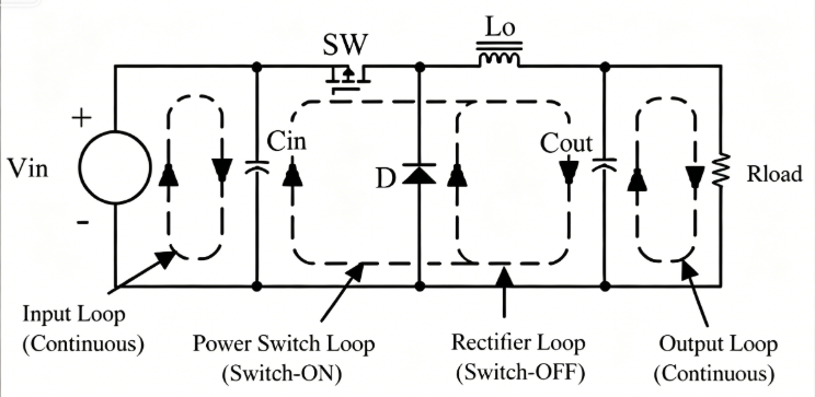
- Switching power supplies usually have 4 current loops: input, output, switching, and freewheeling, as shown in Figure 2. Among them, the input and output current loops are almost DC and generate almost no EMI, but are susceptible to interference; the switching and freewheeling current loops have large di/dt and require attention.
- The gate drive circuits of MOS (IGBT) transistors also usually contain large di/dt.
- Do not place small signal loops, such as control and analog circuits, inside high-current, high-frequency, and high-voltage loops to avoid interference.
- Reduce the loop area and trace length of susceptible (sensitive) signals to minimize interference.
- Keep small signal traces away from large dv/dt signal lines (such as the C or D pole of switching tubes, snubber and clamping networks) to reduce coupling. Ground (or power supply, i.e., constant potential signals) can be poured in the middle to further reduce coupling, and the poured ground should be in good contact with the ground plane. Small signal traces should also be kept away from large di/dt signal lines to prevent inductive crosstalk. Small signal traces should preferably not run below large dv/dt signals. If the back of small signal traces can be poured with ground (same nature ground), it can also reduce the coupled noise signals.
- A better practice is to pour ground around and on the back of these large dv/dt and di/dt signal traces (including the C/D poles of switching devices and switching tube heat sinks), connect the upper and lower ground planes with vias, and connect this ground to the common ground point (usually the E/S pole of the switching tube or the sampling resistor) with a low-impedance trace. This can reduce radiated EMI. Note that the small signal ground must never be connected to this shield ground, otherwise it will introduce significant interference. Large dv/dt traces usually couple interference to heat sinks and nearby ground through mutual capacitance. It is best to connect the switching tube heat sink to the shield ground. Using surface-mount switching devices also reduces mutual capacitance and thus coupling.
- Traces that are prone to interference should preferably not use vias, as they will interfere with all layers that the vias pass through.
- Shielding can reduce radiated EMI, but it increases the capacitance to ground, which will increase conducted EMI (common mode or non-intrinsic differential mode). However, as long as the shield is properly grounded, it will not increase much. Trade-offs can be made in actual design.
- Prevent common impedance interference by adopting single-point grounding and leading out power from a single point.
- Switching power supplies usually have three types of grounds: input power high-current ground, output power high-current ground, and small signal control ground. The ground connection methods are shown in the following schematic diagrams:
- When grounding, first determine the nature of the ground before connecting. The ground for sampling and error amplification should usually be connected to the negative terminal of the output capacitor, and the sampling signal should usually be taken from the positive terminal of the output capacitor. The small signal control ground and drive ground should usually be connected to the E/S pole of the switching tube or the sampling resistor respectively to prevent common impedance interference. Usually, the control ground and drive ground of the IC are not led out separately. In this case, the lead impedance from the sampling resistor to the above grounds must be minimized to maximize the reduction of common impedance interference and improve the accuracy of current sampling.
- The output voltage sampling network is best placed close to the error amplifier rather than the output terminal, because low-impedance signals are less susceptible to interference than high-impedance signals. The sampling trace pairs should be as close to each other as possible to reduce picked-up noise.
- In layout, note that inductors should be kept away from each other and perpendicular to each other to reduce mutual inductance, especially energy storage inductors and filter inductors.
- In layout, note that when high-frequency capacitors and low-frequency capacitors are used in parallel, the high-frequency capacitors should be placed close to the user.
- Low-frequency interference is generally differential mode (below 1M), and high-frequency interference is generally common mode, usually coupled through radiation.
- If high-frequency signals are coupled to the input leads, it is easy to form EMI (common mode). A ferrite bead can be sleeved on the input lead near the power supply. If EMI is reduced, this problem exists. The solution is to reduce coupling or reduce circuit EMI. If high-frequency noise is not filtered out completely and conducted to the input leads, it will also form EMI (differential mode). In this case, sleeving a ferrite bead cannot solve the problem. Connect two high-frequency inductors (symmetrical) in series on the input lead near the power supply. If EMI is reduced, this problem exists. The solution is to improve filtering or use buffering, clamping and other means to reduce the generation of high-frequency noise.
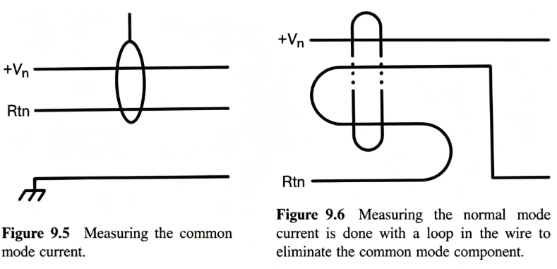
- Measurement of differential mode and common mode currents:
- EMI filters should be placed as close to the incoming line as possible, and the incoming line traces should be as short as possible to minimize the coupling between the front and rear stages of the EMI filter. The incoming line is best shielded with chassis ground (as described above). The output EMI filter should be handled similarly. Keep the distance between the incoming line and high dv/dt signal traces as far as possible, which should be considered in the layout.
About MaxipcbMaxipcb enables advanced electronic innovation. We deliver one-stop solutions including circuit design, simulation, testing, PCB fabrication, component sourcing and SMT&PCBA assembly, to boost R&D efficiency, speed up mass production and control full-cycle risks. We serve global sectors like communication, industrial automation, aerospace, automotive and semiconductor, jointly forging a safer, connected intelligent future.


