Timing is critical in circuit design, and skew (delay difference) is a key factor in signal integrity. Excessive skew causes timing violations and product failure. This article introduces two methods to calculate skew without PCB design tools: using PLTS and ADS.
Timing is critical in circuit design, and skew (delay difference) is a key factor in signal integrity. Excessive skew causes timing violations and product failure. This article introduces two methods to calculate skew without PCB design tools: using PLTS and ADS.
Overview
Physical equal length does not equal equal time delay. Skew can be calculated from S‑parameters, which fully characterize passive interconnects (PCB, connectors, cables, packages).
Method 1: Measure Skew Using PLTS (Physical Layer Test System)
Step-by-Step Operation
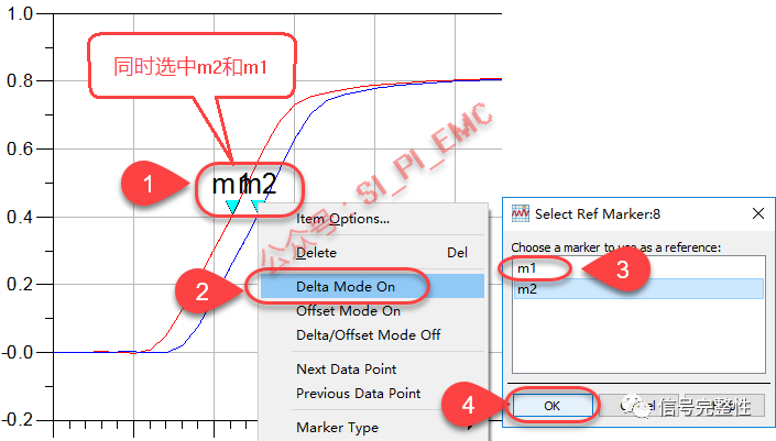
- Import S‑parameters into PLTS.
- Select Time Domain analysis.
- Choose port data (e.g., T21, T43).
- Right‑click → Measure → Skew.
- Enable Skew Measurement to read skew directly.
Result: Skew(T21, T43) = 20.02 ps
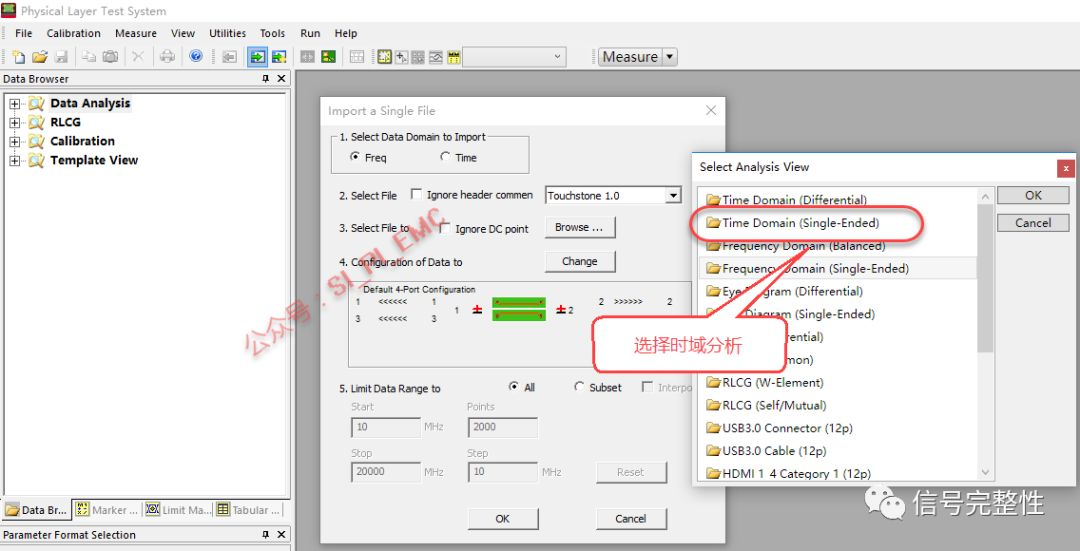
PLTS software interface – S‑parameter import settings
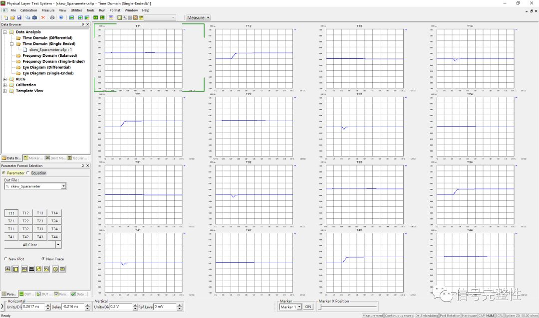
PLTS time‑domain waveform showing T21 and T43 traces
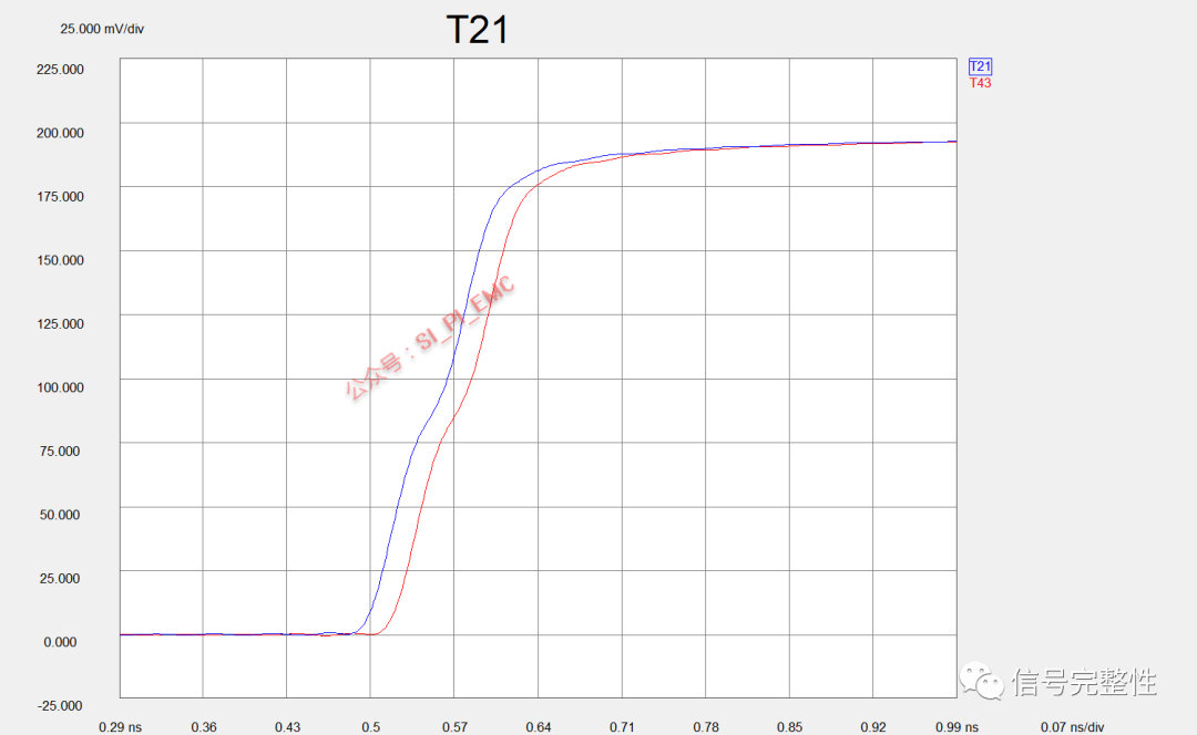
PLTS skew measurement window displaying 20.02 ps
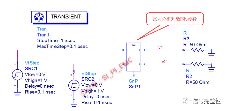
Method 2: Simulate Skew Using ADS (Transient Simulation)
Step-by-Step Operation
- Build schematic with Transient simulator.
- Import the same S‑parameters file.
- Set 50 Ω terminations and pulse sources.
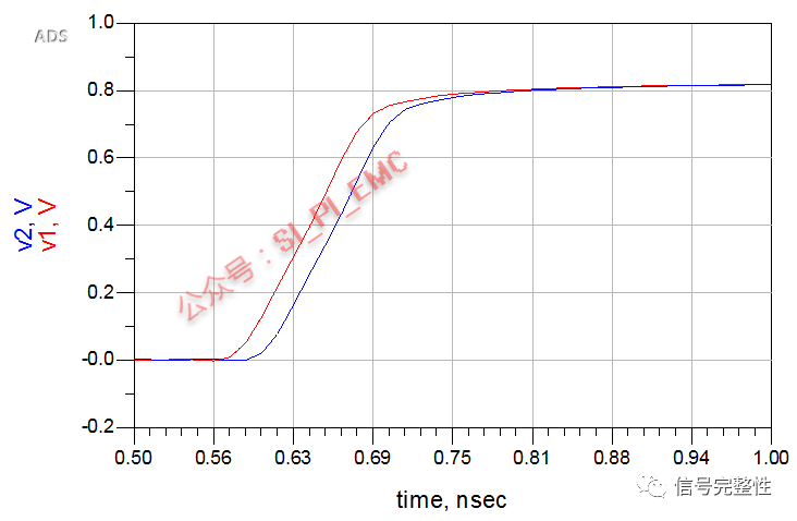
- Run simulation and plot output waveforms v1, v2.
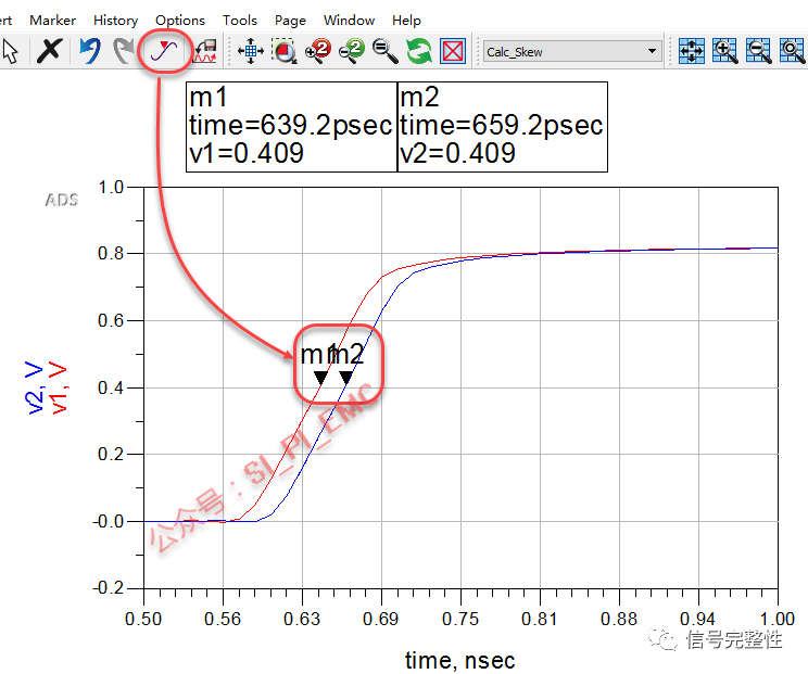
- Place markers at 50% amplitude for both edges.
- Read time difference = skew.
Result: Skew = 20 ps (matches PLTS; slight difference from software rounding)
ADS transient simulation schematic

ADS waveform with markers at 50% amplitude
ADS delta marker showing skew value
Other Measurement Methods
Skew can also be measured directly using:
- Network Analyzer (e.g., E5071C)
- Sampling Oscilloscope
Network analyzer skew measurement screen
Why Control Skew?
- Causes signal integrity degradation
- Increases EMI radiation
- Violates timing margins
Mitigation:
- PCB: length tuning
- Connectors/cables: structural optimization
About Maxipcb
Maxipcb empowers innovators to turn cutting-edge technologies into reality.
We offer one-stop solutions for design, simulation, testing, PCB manufacturing, component procurement and SMT assembly, enabling efficient development, rapid deployment and risk control across the full product lifecycle.Serving the world in communications, industrial automation, aerospace, automotive, semiconductor and beyond, we build a safer, more connected future together.

 PLTS software interface – S‑parameter import settings