Today, we are going to share 8 common markings on PCB boards.

From left to right: Stamp holes - Via types - Solder thief pads - Fiducial marks
From left to right: PCB slotting, PCB conductive keypad, spark gap and fuse trace, with FUSE label
1. PCB Stamp Holes
During panelization, to facilitate the separation of individual PCB boards, a small contact area is reserved between the boards, with holes in this area called stamp holes. Personally, I think the name "stamp holes" comes from the serrated edge left after separating the PCBs, which looks just like the perforated edge of a postage stamp.
2. PCB Via Types
In many cases, you will see mounting holes surrounded by tiny vias. There are two main types of mounting holes: plated and non-plated. There are two main reasons for using surrounding vias:
- When we need to connect the hole to inner layers (such as GND in a multilayer PCB);
- For non-plated holes, when we need to connect the top and bottom pads.
3. Solder Thief Pads
One of the common defects in wave soldering is solder bridging during the soldering of SMD components. As a solution, engineers found that adding an extra pad at the end of the original pins can solve this problem. The width of the extra pad is 2-3 times that of a standard pad. It is also known as a solder thief, as it absorbs excess solder and prevents solder bridging.
4. Fiducial Marks (Mark Point Marking)
A fiducial mark consists of a bare copper circle inside a larger bare circular keep-out area. This fiducial mark is used as a reference point for pick-and-place (PnP) machines. Fiducial marks are placed in three positions:
- On the whole panel;
- Beside fine-pitch components such as QFN and TQFP;
- At the corners of the PCB.
5. Spark Gap
Spark gaps are used for ESD, current surge and overvoltage protection. High voltage will ionize the air between the two terminals, and a spark will form between them before the high voltage damages the rest of the circuit. This protection method is not recommended, but it is better than no protection at all. Its main disadvantage is that its performance will degrade over time. The breakdown voltage can be calculated by the following formula:
V=((3000×p×d)+1350)
Where "p" is the atmospheric pressure, and "d" is the distance in millimeters.
6. PCB Conductive Keypad
If you have taken apart a remote control or a calculator, you must have seen this marking. A conductive keypad consists of two interlaced but unconnected terminals. When the rubber button on the keyboard is pressed, the two terminals are connected, as the bottom of the rubber button is conductive.
7. Fuse Trace
Similar to the spark gap, this is another low-cost technique implemented on the PCB. A fuse trace is a necked-down trace on the power line, acting as a one-time fuse. The same configuration can be used as a PCB jumper, where a specific connection is removed by simply etching away the necked trace (PCB jumpers can be found on the reset line of some Arduino UNO boards).
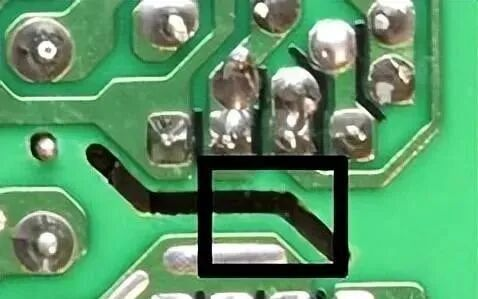
8. PCB Slotting
If you look at PCBs in high-voltage equipment such as power supplies, you may notice air slots between certain traces. Intermittent arcing in PCBs will cause carbonization of the PCB, which in turn leads to short circuits. For this reason, routing slots can be added in the suspected area, where arcing may still occur but will not cause carbonization.
 About Maxipcb
Maxipcb empowers innovators to turn cutting-edge technologies into reality.
We offer one-stop solutions for design, simulation, testing, PCB manufacturing, component procurement and SMT assembly, enabling efficient development, rapid deployment and risk control across the full product lifecycle.Serving the world in communications, industrial automation, aerospace, automotive, semiconductor and beyond, we build a safer, more connected future together.


