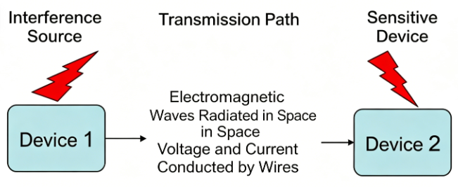
High-speed signal lines, IC pins, and connectors can act as radiation interference sources, emitting electromagnetic waves to disrupt the normal operation of systems or sub-systems.
Core Definitions
- ESD (Electro-Static Discharge): A natural phenomenon of static electricity release, characterized by high voltage, low power, small current, and short action time, which easily causes instability or damage to electronic products.
- EMI (Electromagnetic Interference): High-speed signal lines, IC pins, and connectors can act as radiation interference sources, emitting electromagnetic waves to disrupt the normal operation of systems or sub-systems.
1. ESD Protection Design
- Structural Isolation: Recess connectors into the housing to lengthen the static discharge path and weaken energy.
- Sensitive Device Protection: Add shielding covers for sensitive modules (RF, audio, memory).
- Core Component Layout: Place the RK3588 chip and core parts in the center of the PCB; ensure shielding covers are at least 2mm from the board edge and reliably grounded.
- Modular Layout: Arrange components by functional modules and signal flow; isolate interference sources (e.g., DC-DC switching power supplies).
- ESD Device Placement: Install ESD components at interfaces or static discharge points; route signals through ESD devices before drilling vias.
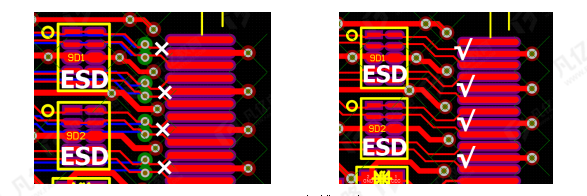
- Spacing Rules: Keep components ≥20mil from the board edge and ≥40mil from connectors.
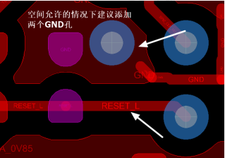
- Grounding Design: Provide a complete GND loop on the surface layer; connect connectors and shielding covers to the surface ground with multiple ground vias at welding points; avoid routing or cutting ground copper near connectors.
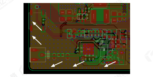
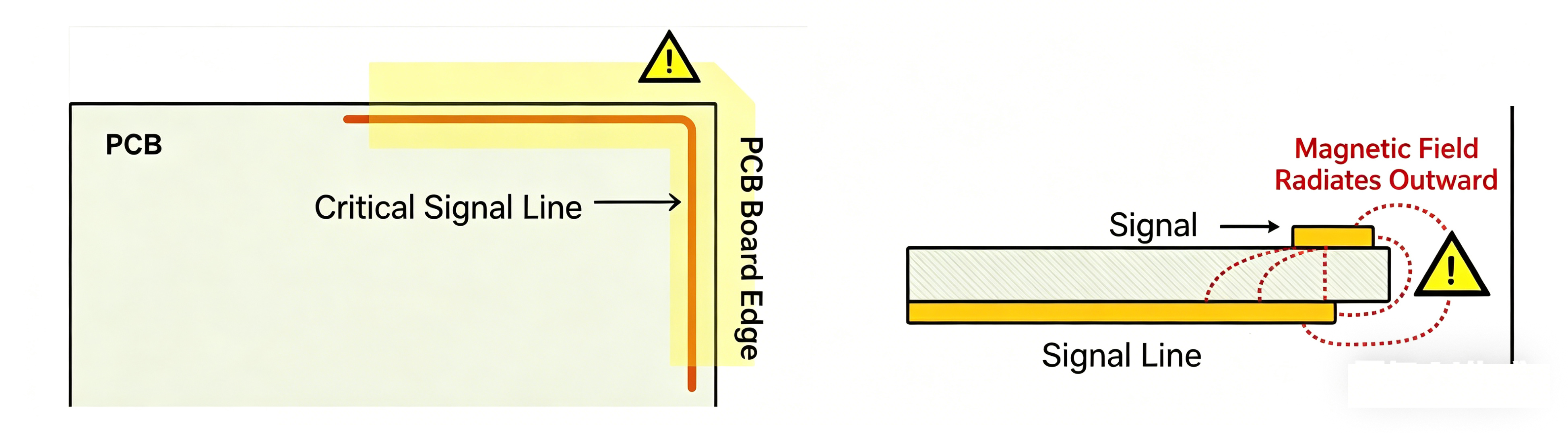
- Board Edge Treatment: Do not route signals on the surface board edge; add plenty of ground vias and isolate signals from ground if needed.
- Copper Exposure: Expose copper in blank PCB areas to enhance static discharge.
- Board-to-Board Connection: Series 2.2–10Ω resistors for signals and reserve TVS devices to improve anti-static surge capability.
- RK3588 nPOR Pin: Place a 100nF capacitor close to the pin with at least one 8/16mil ground via (two or more if space allows).
- Critical Signals: Keep reset, clock, interrupt signals ≥5mm from the board edge; provide a reference plane under routing to avoid edge effects.
- Peripheral Chip Reset Pins: Add a 100nF capacitor close to the pin with ground vias for reliable grounding.
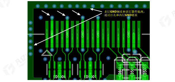
- Regional Isolation: Use independent vias for connector ground pins to connect inner ground layers; isolate sensitive signals from static discharge areas on the surface layer.
2. EMI Protection Design
- Interference Control: Address EMI by suppressing interference sources and cutting off coupling paths (the three elements of EMI: interference source, coupling channel, sensitive equipment).
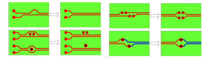
- Suppression Methods: Use filtering, grounding, impedance control, and termination; reliable grounding is fundamental.
- EMI Components: Shielding covers, filters, resistors, capacitors, inductors, ferrite beads, common-mode chokes, wave-absorbing materials, and spread-spectrum devices.
- Filter Selection: Use capacitive filters for high-impedance loads and inductive filters for low-impedance loads; apply common-mode chokes for differential interfaces.
- Shielding Grounding: Ensure shielding structures are well-grounded to avoid radiation leakage or antenna effects.
- Spread-Spectrum Clocking: Use module-level spread-spectrum for RK3588 per signal requirements.
- Clock Matching: Retain series matching resistors for clocks and place them close to the CPU (routing ≤400mil).
- Power Input Filtering: Reserve common-mode inductors or EMI filters at power inputs.
- Interface Filtering: Add common-mode inductors or filter circuits for USB, HDMI, VGA, and display connectors.
- Heatsink Design: Select heatsinks that meet both thermal and EMI requirements; reserve grounding points.
- Common Rules with ESD: Most ESD layout rules apply to EMI; ensure signal integrity and symmetric, length-matched differential routing.
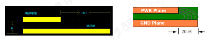
- Layer Design: Route clocks on inner layers for PCBs with ≥4 layers; follow the 20H rule (power plane retracted by 1mm from the ground plane) to reduce radiation.
About Maxipcb
Maxipcb empowers innovators to turn cutting-edge technologies into reality.
We offer one-stop solutions for design, simulation, testing, PCB manufacturing, component procurement and SMT assembly, enabling efficient development, rapid deployment and risk control across the full product lifecycle.Serving the world in communications, industrial automation, aerospace, automotive, semiconductor and beyond, we build a safer, more connected future together.


