As the industry begins mass production of next-generation PoP devices, the process and material standards for surface mount assembly and PoP assembly must be upgraded accordingly.
As the industry begins mass production of next-generation PoP devices, the process and material standards for surface mount assembly and PoP assembly must be upgraded accordingly.
When Apple’s iPhone debuted in 2007 and was quickly disassembled for public display, Package-on-Package (PoP) technology re-entered the spotlight. PoP was once a major focus of industry attention, yet it faded from view for a considerable period. At present, as advanced smartphones integrate processors and memory, PoP has once again become the packaging solution of choice for such devices.
After several years of steady development, all major mobile phone manufacturers have adopted PoP architectures, which serve as the core technology driving their flagship products. This shift stems not only from visible advantages in size and performance but also from less obvious commercial and supply chain factors. PoP has a promising future, as it is being adopted in numerous new products that demand ever-improving performance, smaller form factors, and diverse memory configurations and interfaces. Diversified PoP solutions are advancing rapidly to meet growing market demands. Having proven its maturity, PoP is now being adopted in applications beyond mobile phones.
Notably, Texas Instruments and Nokia were the first to recognize the potential of PoP and implement large-scale production. Printed Circuit Boards (PCBs) in mobile phones always integrate memory and processors. In the past, these components were individually packaged and placed side by side. Consumer demand for the latest feature-rich applications in mobile phones requires increasing memory capacity, creating an urgent need to stack memory devices within the same package size and form factor. This approach has achieved great success. As a result, nearly every mobile phone today contains at least one die-stacked package, and this trend is steadily growing.
Stacking memory on logic devices may seem logical for achieving greater miniaturization, performance, and cost efficiency. However, this seemingly straightforward approach is far from simple. Logic processors are high-value components in logic-plus-memory configurations or stacks, and logic device manufacturers face significant challenges when integrating their logic devices with memory devices. They typically source memory in wafer form, which is not their core product, making them highly concerned about memory test yield, interaction, and quality. Moreover, memory testing is highly specialized and best performed by memory manufacturers with full access to test results, avoiding unforeseen complexity and high costs. After several unsuccessful early attempts, most logic device manufacturers seeking to integrate logic and memory in a single package have urgently sought better solutions.
PoP Solution
PoP is recognized as a superior solution for integrating logic and memory devices within a single assembly (Figure 1). The bottom PoP package accommodates logic devices, and its bottom surface supports high pin counts with fine solder ball pitch. The top PoP package holds memory devices or stacked memory components. Since memory devices generally require fewer pins, interconnection can be achieved via a peripheral array at the package edge where the two packages interconnect. The bottom package is manufactured and tested by logic device manufacturers, leveraging their core capabilities and technologies. Liability issues associated with integrating foreign chips in a single package are eliminated, as each manufacturer is only responsible for its own package. End users and mobile device manufacturers benefit from configuration flexibility: traditional memory suppliers provide the top package, while logic device suppliers deliver the bottom package. This setup offers flexible configuration with multiple memory sources and package types, compatible with various processor package types and suppliers.
When logic and memory devices are integrated into the same stacked package, mobile phone manufacturers no longer need to specify fixed component combinations. JEDEC electrical standards (dependent on internal memory configuration) and mechanical standards enable flexible pairing of top memory packages with bottom logic packages. The bottom package also complies with JEDEC mechanical standards. Such standardization allows manufacturers to design and produce mutually compatible products, a key reason why PoP has matured and entered high-volume mass production in recent years.
Today, mass-producing PoP remains challenging, as with all advanced packaging technologies. Many obstacles must be overcome. To realize a flexible PoP structure, the stacked packages must be molded and reflowed simultaneously on the PCB. This was previously difficult to achieve and required development and optimization by mobile phone manufacturers or their Electronics Manufacturing Services (EMS) providers (substrate assembly). Reflowing two Ball Grid Array (BGA) packages stacked on top of each other is challenging, especially for thin, relatively large, fine-pitch BGAs. With narrow package-to-package interconnection pitch (typically 0.65 mm or smaller), the allowable warpage during reflow is extremely limited. Historically, package warpage during reflow was not a primary factor affecting surface mount yield.
Package warpage can now be measured and controlled. A further complication is the difficulty of controlling warpage in the bottom PoP package. The perimeter of the bottom PoP lacks molding compound to enable interconnection with the top package, leaving an unsupported substrate edge. To reduce the overall height of the PoP stack, the substrate is made as thin as possible. The substrate expands under reflow temperatures (all PoP packages use lead-free solder balls at higher reflow temperatures instead of eutectic Sn-Pb solder), inherently causing warpage. Package size, device size, substrate thickness and material, molding compound, die attach thickness, and adhesive material all play critical roles in determining bottom PoP warpage. These parameters must be optimized to produce bottom PoP packages that meet surface mount yield requirements. Generally, PoP stacks that fail reflow onto the PCB cannot be reworked, so first-pass yield in substrate assembly must be extremely high.
Controlling warpage in the top package is also challenging. The top PoP can stack 2 to 5 dies. These devices vary in size; some have identical or similar dimensions, requiring spacers between stacked dies to enable wire bonding to the substrate. While the bottom PoP typically exhibits concave warpage during reflow, the top PoP may warp either concave or convex. Although the top PoP extends molding compound to the package edge and generally exhibits less warpage than the bottom PoP, its warpage must accommodate or compensate for the higher warpage of the bottom package. Optimization of packaging materials and thickness is critical for achieving acceptable surface mount yield for the top PoP. Initial warpage targets for top and bottom packages during reflow were approximately 80 μm. However, extensive research has led some customers to reduce warpage targets to 60 μm for 0.65 mm package-to-package interconnection pitch.
Current PoP Trends and Advancements
Current trends favor smaller, higher-density PoP packages with 0.5 mm package-to-package interconnection pitch, requiring warpage control as low as 50 μm during reflow. These packages will also shift the solder ball pitch on the bottom of the bottom PoP to 0.4 mm. Driven by high pin counts and limited package area (target size typically 12×12 mm or smaller), packages must meet coplanarity specifications at room temperature and strict warpage specifications above the solder melting temperature during reflow. On the surface mount side, improved surface mount processes are being introduced to enable simultaneous assembly and reflow of fine-pitch PoP packages. Typical current surface mount processes include solder paste printing on the PCB, placement of the bottom PoP, dipping of top PoP solder balls in flux, placement of the top PoP on the bottom PoP, and reflow in a clean, dry air furnace. New processes involve dipping top package solder balls in flux or solder paste, enhancing the robustness of top-to-bottom package interconnections during reflow.
Improvements to surface mount and PoP assembly processes and materials are essential as the industry ramps up mass production of next-generation PoP devices. Most bottom packages produced today use wire bond interconnections. However, flip-chip technology meets the 12×12 mm or smaller size requirement while supporting the higher density and performance demands of next-generation packages (Figure 3). Consequently, most bottom PoP logic devices on PCBs are flip-chip devices. Another advantage of flip-chip is that the assembly height is lower than that of molded wire-bond devices. Flip-chip devices do not require molding, reducing manufacturing costs. However, the absence of molding compound and underfill in flip-chip devices creates significant challenges for warpage control.
Controlling Package Warpage
To control package warpage, thicker substrates and new packaging materials are being evaluated. Flip-chip dies can be thinned to meet the maximum assembly height of 0.22 mm (JEDEC mechanical standard), enabling assembly of a top PoP with 0.5 mm pitch on top. Other bottom PoP variants are being developed to improve warpage control and accommodate thicker dies. Currently developed bottom packages feature flip-chip dies with molding compound at the center or extended to the package edge. These packages typically include built-in interconnection vias around the top perimeter (solder on pads or alternative schemes) to “bridge the gap” with the top PoP. This bridging approach is also adopted for bottom packages with two stacked dies. Some advanced next-generation PoP applications require stacking logic-on-logic or logic-on-analog devices. In such stacks, the bottom die uses flip-chip or wire bonding, while the top die always uses wire bonding, necessitating molded packaging. A bridging scheme is mandatory unless the top PoP uses 0.65 mm solder ball pitch.
Height Reduction
Reducing stack height is one of the most difficult challenges facing PoP technology today. Currently, PoP is typically the thickest package in the digital section or on the PCB of mobile phones. While other packages (including die-stacked packages) achieve maximum heights of 1.2 mm or lower, PoP stacks are striving to meet a maximum height of 1.4 mm. Early PoP stacks had maximum heights near 1.8 mm; current PoP stacks are limited to 1.6 mm. The difficulty in reducing stack height lies in lowering device assembly height or the clearance required for molding between bottom packages. As discussed earlier, reducing thickness increases warpage. Top PoP packages can be thinned, but high-volume production uses ultra-thin substrates and dies (substrate thickness 0.13 mm, die thickness 60 to 75 μm). Further reduction requires even thinner substrates, die attach materials (die attach films), and die thickness below 60 μm. These materials typically incur additional costs, and handling such ultra-thin materials and devices in production is problematic.
In recent years, new PoP solutions have been introduced that stack two memory devices in the top PoP while meeting the 1.4 mm maximum height requirement. In the future, such PoP stacks will use ultra-thin memory dies and advanced ultra-thin packaging materials to achieve a maximum height of 1.2 mm.
The Future of PoP
New PoP variants are emerging to address weaknesses of traditional PoP. For example, as packages become thinner and solder ball pitch finer, one solution to PoP warpage challenges is to pre-assemble the top and bottom packages before mounting to the PCB. While this reduces PoP’s flexibility advantage, pre-stacking before substrate assembly is a relatively simple process with easier warpage control during reflow (independent of PCB warpage). Pre-stacked PoP can be tested to ensure functionality and exhibits lower warpage than separate top or bottom PoP packages, making PoP assembly similar to mounting conventional fine-pitch BGAs on the PCB. Pre-stacked PoP is attractive to device manufacturers that can now offer end customers low-end logic devices paired with top memory packages. This option appeals to customers adopting PoP for their products rather than to end users of mobile handsets.
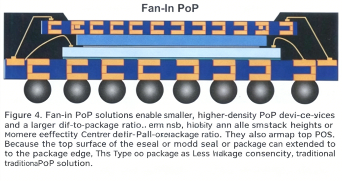
As processor performance and capacity in bottom PoP packages continue to increase, die sizes grow larger—even as wafer process geometries shrink from 90 nm to 65 nm and below. This makes it difficult to fit devices within the required 12×12 mm or smaller package size. Fan-in PoP solutions (with pads on the top surface of the bottom PoP located at the center instead of the perimeter) are being developed to enable smaller, higher-density PoP devices and higher die-to-package ratios (Figure 4). Fan-in PoP also enables smaller, cost-effective top PoP packages with central BGA arrays. Since molding compound or the top package surface extends to the package edge, such packages exhibit lower warpage than traditional PoP solutions. Another advantage of fan-in PoP is its ability to support a higher number of interconnections on the top stacked package without increasing package size, thanks to a central interconnection array with 0.5 mm or even 0.4 mm pitch. This enables processor-to-processor package stacking or processor-to-high-pin-count memory interfaces, a key technology for mobile phone manufacturers. In a sense, PoP variants such as fan-in PoP are assuming the role of embedded components in substrates, while fan-out wafer-level packaging aims to address future needs.
Conclusion
PoP has existed for a long time as a packaging format but will become the mainstream packaging solution for integrating processors and memory in mobile phones for years to come. Many new products will launch with PoP, and new PoP variants will meet demands for smaller size, lower profile, higher performance, finer solder ball pitch, and increased pin counts. The introduction and improvement of new materials will effectively mitigate package warpage, and advanced surface mount technologies will help achieve required board-level assembly yields. PoP is expanding from mobile phone applications to other handheld devices and memory applications, and this trend is likely to continue. Therefore, PoP will remain at the forefront of 3D packaging innovation.
About Maxipcb
Maxipcb enables advanced electronic innovation. We deliver one-stop solutions including circuit design, simulation, testing, PCB fabrication, component sourcing and SMT&PCBA assembly, to boost R&D efficiency, speed up mass production and control full-cycle risks. We serve global sectors like communication, industrial automation, aerospace, automotive and semiconductor, jointly forging a safer, connected intelligent future.


