Detailed explanation of PCB process route: additive process vs reduction method, understand the core differences and future trends in one article.
Detailed explanation of PCB process route: additive process vs reduction method, understand the core differences and future trends in one article.
"With the continuous evolution of electronic products in the direction of high density, thinness and high performance, PCB manufacturing technology as its core is also facing new challenges and opportunities. Among many technological routes, the traditional "reduction method" and the emerging "additive process" are the two core technological paths. This article will provide you with a systematic and in-depth comparative analysis from technical principles, cost structure to application selection. "
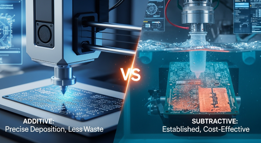 1, the fundamental difference of technical principle
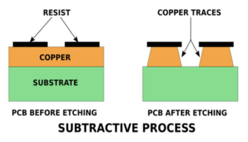
1.1 Subtractive Process.Additive process process takes copper clad laminate as the base material, and removes the unnecessary copper layer by chemical etching (such as acidic or alkaline solution), thus retaining the designed circuit pattern.
Key steps:
Cutting and surface treatment of copper clad laminate
Graphic transfer (film pasting, exposure and development)
Use acidic/alkaline etchant to remove excess copper foil.
Solder Resisting Layer and Character Screen Printing
Features: The conductive path is formed by the "subtraction" of copper layer, and the etching parameters need to be accurately controlled to avoid over-etching or copper residue.
 1.2 Additive Process process (additive process)
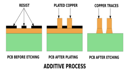
Additive process process directly deposits conductive materials (such as copper and silver paste) on the insulating substrate, and builds circuits layer by layer.
Key steps:
Pretreatment of bare substrates (such as polyimide and ceramics)
Selectively applying photoresist or electroplating to deposit the conductive layer.
Drying, curing and removing excess materials.
Features: Fine lines can be directly formed without etching, which is suitable for micro-pitch and high-density design.
 2, process flow comparison
| Step |
Reduction process |
Additive process craft |
| Material preparation |
Copper clad laminate (copper foil+resin substrate) |
Bare substrate (such as polyimide film) |
| Graphic transfer |
Coating photoresist → exposure → development → etching. |
Coating photoresist → exposure → development → electroplating. |
| Line formation |
Reduce the thickness of copper layer |
Increase conductive material |
| aftertreatment |
Solder resist printing and surface treatment (OSP/HASL) |
Solder resist printing and surface treatment (OSP/HASL) |
- Reduction method: consumer electronics motherboard, home appliance control panel
- Additive process: flexible medical sensor, high frequency microwave substrate.
3. Core advantages and limitations3.1 the competitive advantage of the reduction methodAdvantages:
High technology maturity: occupying more than 80% market share and perfect supply chain.
Good cost-effectiveness in mass production: suitable for large-scale production of single/double panels.
Excellent thermal performance: thick copper layer can support high current applications.
Limitations:
The pressure of environmental protection is great: the treatment cost of etching wastewater is high.
Line width/line spacing limit: the limit is about 20μm, which is not suitable for ultra-high density requirements.
Poor flexibility: not suitable for folding equipment.
3.2 additive process's breakthrough pointAdvantages:
Ultra-fine machining: the line width can be less than 5μm, which supports IC carrier-level accuracy.
Green manufacturing: no copper etching waste, in line with RoHS/REACH standards.
Adapt to complex structure: 3D curved surface and through-hole circuit can be realized.
Limitations:
High equipment cost: electroplating bath, vacuum deposition machine and other equipment are expensive.
Material limitation: limited to nonmetallic substrates (such as ceramics and polymers).
Low mass production efficiency: suitable for small batch and prototyping.
4. Deep analysis of cost structure4.1 Cost model of reduction methodFixed cost: etching machine, depreciation of exposure equipment (accounting for 30% of the total cost).
Variable cost:
Copper foil waste: The thinner the line width, the higher the scrap rate (for every 0.1mm reduction, the scrap rate will increase by 5%).
Etchant consumption: the cost of ferric nitrate solution is about $5/kg, and the dosage is 10L per hour.
Wastewater treatment: about $0.8 per square meter of PCB.
Case study:
Production of 1㎡ 4-layer FR4 board (100μm line width);
Material cost: $12
Processing cost: $8 (including etching and drilling)
Total cost: $20
4.2 additive process cost modelFixed costs: plating equipment and clean room maintenance (accounting for 45% of the total cost).
Variable cost:
Conductive material: nano-silver paste $50/g, 0.1g per layer.
Energy consumption: electroplating bath power is 5kW, and the operating cost is $0.15/h.
Yield loss: the yield of complex structure is about 75% (92% by reduction method).
Case study:
Production of 1㎡ 6-layer ceramic substrate (20μm line width);
Material cost: $35
Processing cost: $18 (including sputtering and electroplating)
Total cost: $53
Cost breakeven point analysis:
For batch orders larger than 500㎡, the cost of reduction method is 35% lower. For small batch (< 100m2), additive process premium can reach 200%.
5, six key application scenarios decision guide
| scene |
Recommended process |
Key reason |
| Consumer electronics motherboard |
Reduction method |
Mass production, low cost and mature technology. |
| 5G base station high frequency PCB |
Additive process |
Low dielectric loss, supporting millimeter wave frequency. |
| Flexible circuit of wearable device |
Additive process |
Bending times > 100,000 times, thickness < 0.1 mm. |
| Automobile control module |
Reduction method |
High temperature resistance (150°C), vibration resistance |
| Semiconductor package substrate |
Additive process |
Line width/line spacing ≤50μm, supporting TSV 3D packaging. |
| Military/aviation high reliability PCB |
Reduction method |
Passed MIL-STD-883 certification |
Laser Direct Forming (LDS): Selective copper plating is realized by laser activation.
Green etchant: adopt nitrate-free sodium persulfate system to reduce pollution.
6.2 additive process Process BreakthroughRoll-to-roll (R2R) production: continuous manufacturing of flexible substrates is realized.
3D printing conductive ink: nano silver/copper particles are written directly, and the accuracy can reach 10 μ m.
6.3 mixing processCombination of material reduction and material addition: reduction method is used for the main line, and additive process is used for the micro-through hole.
Metal organic chemical vapor deposition (MOCVD): copper nanowire network is grown on the substrate.
Concluding remarksChoosing PCB technology is essentially a trade-off between three dimensions: cost, accuracy and output. With the development of semiconductor packaging towards 2.5D/3D, additive process will be more adopted in high-end applications; The reduction method will still occupy a dominant position in the traditional market with its mature ecosystem. Enterprises must establish a process evaluation matrix and dynamically adjust the strategy according to the product life cycle (PLM) data. For engineers, mastering the collaborative design ability of the two processes will be the core competitiveness to meet the challenges of the next generation of electronic products.
About MaxipcbMaxipcb inspires and empowers innovators and helps them bring world-changing technologies to life. We provide advanced design, simulation and testing solutions to help engineers complete development and deployment faster in the whole product life cycle, while controlling risks. Our customers are all over the world, such as communication, industrial automation, aerospace and national defense, automobile, semiconductor and general electronics. We join hands with customers to accelerate innovation and create a safe and interconnected world. 
