1. Add a Common Ground Plane Under Signal Traces
Add a common ground plane beneath signal traces to minimize the impedance between any two grounding points on the PCB.
When the outer layer close to the ground plane is used for mounting high-speed components (e.g., RF components with microstrip or coplanar lines), the other side can be used for less critical components. The second inner layer serves as the power plane, which should be as large as possible to reduce impedance.
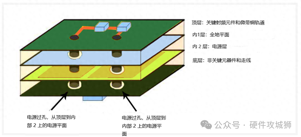
Layer stackup with a common ground plane under signal traces
For cost reduction, a double-sided PCB is preferable, with ground planes added on both sides of the traces interconnected by a large number of vias.
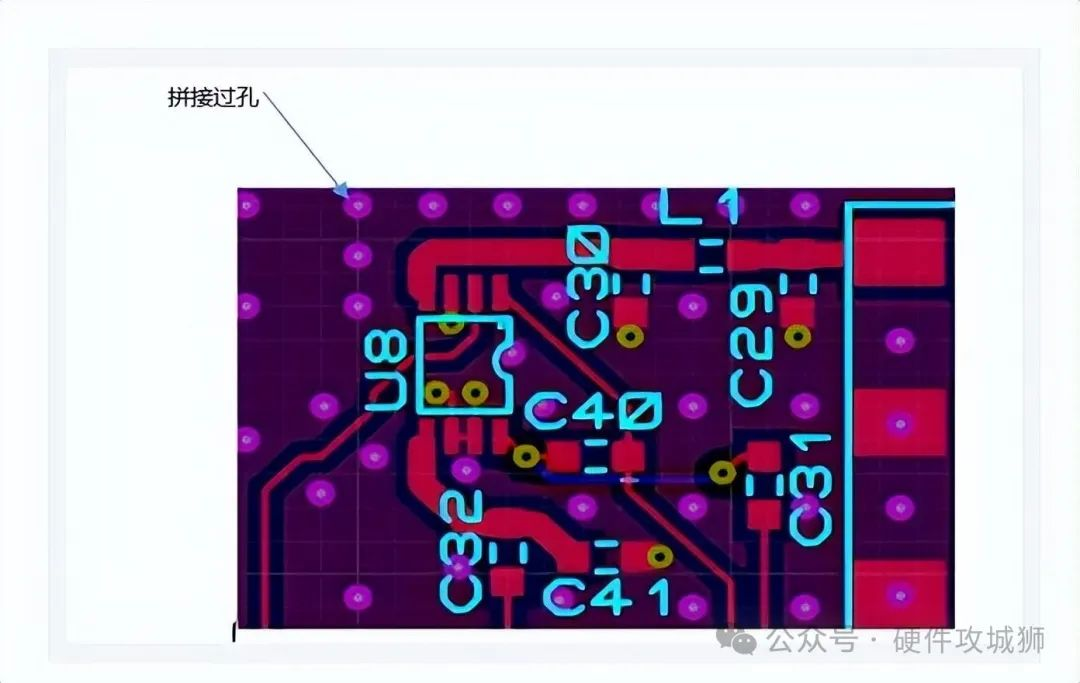
Double-sided PCB with vias for stitching ground planes
Isolated ground planes for single-point interconnected digital and analog components can reduce ground plane noise. Traces from one area to another should all be routed above the interconnection point; otherwise, antenna-like structures may form, emitting or receiving spurious signals. A single, continuous ground plane is recommended.
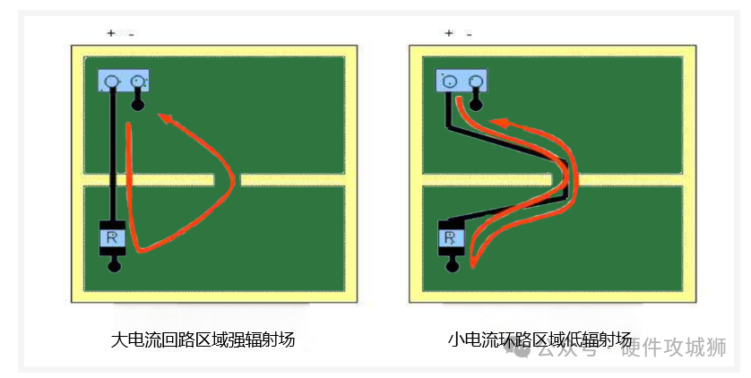
Radiation fields of different current loop areas
2. Add Vias in a Grid to Avoid Hot Spots
Signal vias create gaps in power and ground planes. Improper via placement leads to plane areas with increased current density, known as hot spots.
The best way to avoid hot spots is to place vias in a grid with sufficient space between them for power plane routing (a 15-mil via pitch is recommended).
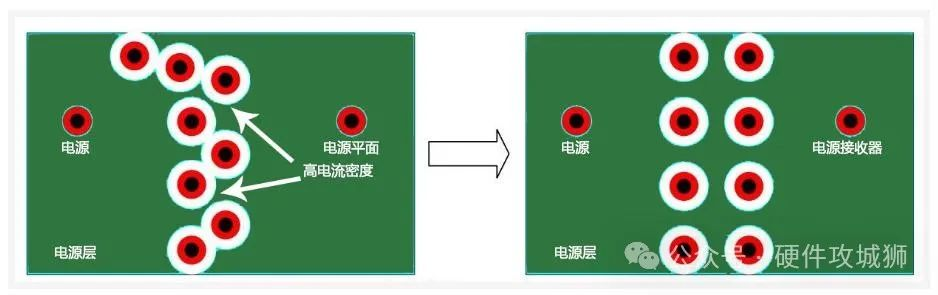
Via placement in a grid to avoid hot spots
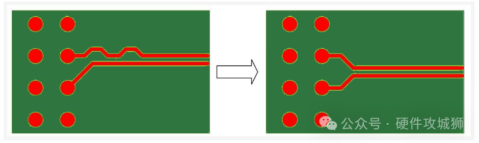
3. Use 135° Bends Instead of 90° Bends for High-Speed Signal Routing
Minimize bends when routing high-speed signals; use 135° bends if a bend is necessary, instead of 90° bends.
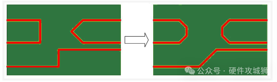
135° bends vs 90° bends for high-speed signals
90° bends cause inconsistent PCB etching, and their sharp edges act as antennas for high-speed signals.
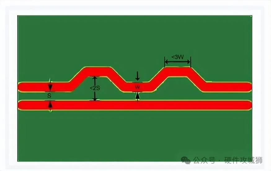
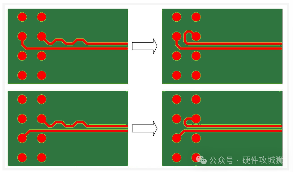
For specific trace length requirements, serpentine routing is used. The minimum distance between adjacent copper segments of the same trace must be 4 times the trace width, and each bend segment should be 1.5 times the trace width.
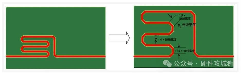
Minimum distance and segment length for serpentine routing bends
4. Increase Spacing Between Signals Outside Bottleneck Zones to Avoid Crosstalk
Maintain a minimum distance between traces to minimize crosstalk, whose level depends on the length and spacing of the two traces. In bottleneck zones where traces are routed closer than expected, increase the spacing between additional signals beyond the minimum requirement.
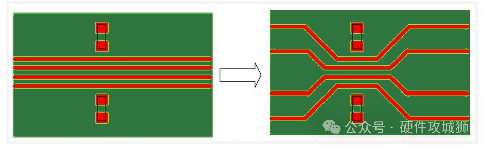
Maximize trace spacing to avoid crosstalk
5. Use Daisy Chaining to Preserve Signal Integrity and Avoid Stub Traces
Long stub traces can act as antennas, increasing EMC compliance issues, and generate reflections that negatively impact signal integrity. Pull-up or pull-down resistors on high-speed signals are common sources of stubs. If such resistors are required, route the signal in a daisy chain.
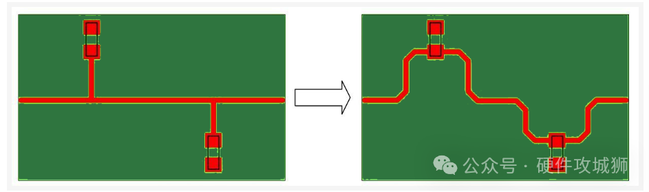
Daisy chaining to eliminate stub traces
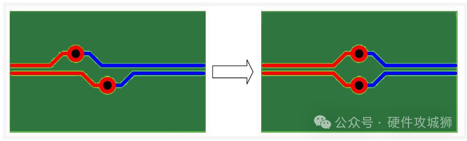
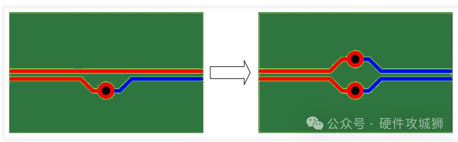
6. Do Not Place Components or Vias Between Differential Pairs
Route high-speed differential pairs in parallel with a constant spacing to achieve the specified differential impedance. Minimize areas where the specified spacing is widened due to pad entry, and route differential pairs symmetrically.
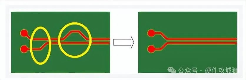
Symmetric routing of differential pairs with parallel signals
Never place any components or vias between differential pairs, even if the signals are routed symmetrically.
Prohibition of component/via placement between differential pairs
Placing components/vias between differential pairs may cause EMC issues and impedance discontinuities.
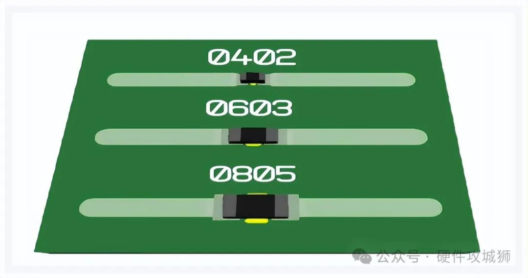
Some high-speed differential pairs require series coupling capacitors, which must be placed symmetrically. Capacitors and their pads introduce impedance discontinuities; use 0402 or 0603 capacitor sizes and avoid larger packages such as 0805 or type C.
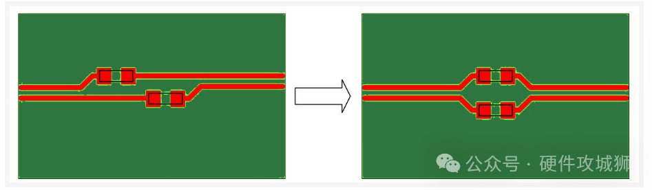
Symmetric placement of coupling capacitors for differential pairs
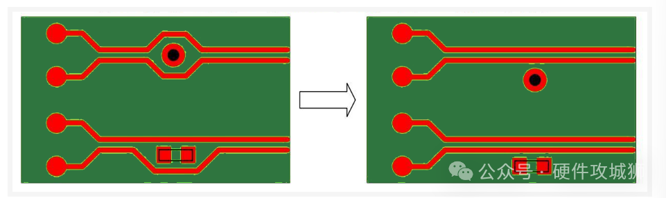
Vias introduce significant impedance discontinuities, so minimize their number and place them symmetrically.
Symmetric placement of vias for differential pairs
Route the two traces of a differential pair on the same layer to meet impedance requirements, and include the same number of vias for both traces.
Differential pair routing on the same layer with equal number of vias
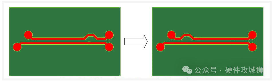
7. Implement Length Matching for Tight Skew Between Positive and Negative Signals
High-speed interfaces have strict timing requirements for signal arrival at the destination, known as clock skew between different traces and signal pairs. For example, in high-speed parallel buses, all data signals must arrive within a specific time window to meet the receiver’s setup and hold time requirements.
Differential pair signals require extremely small skew between positive and negative traces. Use serpentine routing to compensate for length differences, and carefully design the serpentine geometry to reduce impedance discontinuities.
Recommended serpentine routing geometry for length matching
Place serpentine routing at the root of length mismatches to ensure synchronous propagation of positive and negative signal components through the connection.
Length correction at the source of mismatches
Bends are a common source of length mismatch; place compensators as close to bends as possible (maximum 15mm distance).
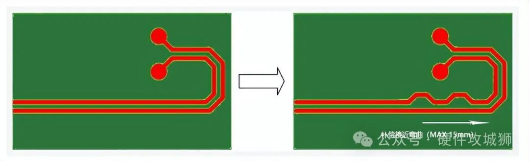
Placing length compensators near bends
Two bends often compensate for each other; no additional serpentine compensation is needed if the bends are less than 15mm apart. The asynchronous transmission distance of signals should not exceed 5mm.
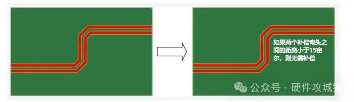
Mutual compensation of adjacent bends
Compensate for mismatches individually at each stage of differential pair connections. If vias split a differential pair into two segments, compensate for bends in each segment separately to ensure synchronous propagation through the vias.
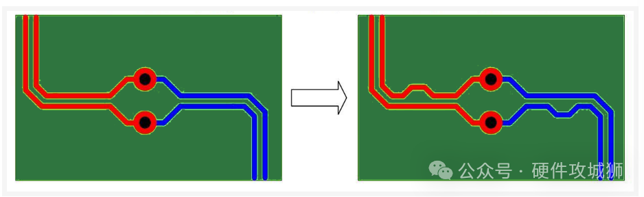
Individual length compensation for each differential pair segment
Signal speeds vary across PCB layers; for length matching, route traces on the same layer (as the speed difference is difficult to quantify).
Routing signal pairs of the same interface on the same layer
Some CAD tools include the internal trace length within capacitor pads in length calculations, showing a length difference between positive and negative signals even if the internal traces are unused. To minimize this, ensure equal pad entry for both signals.
Length calculation issues in CAD tools (capacitor pad internal traces)
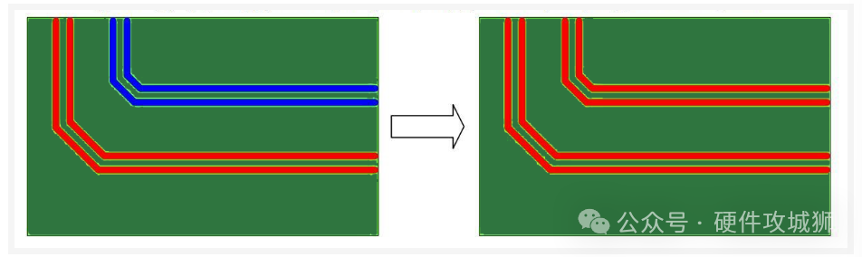
Asymmetric fanout is preferred for differential pair signals to avoid serpentine routing as much as possible.
Asymmetric fanout for differential pairs
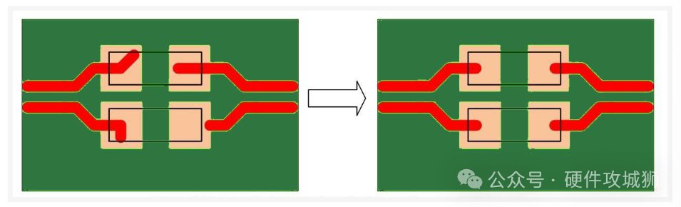
If there is sufficient space between pads, add small loops for shorter traces instead of serpentine routing; vias are preferable to serpentine routing for length compensation.
Preferred fanout for differential pairs (small loops instead of serpentine)
8. Do Not Route Signals Over Split Planes
Incorrect signal return paths cause noise coupling and EMI issues. Designers must always consider the signal return path when routing. While power rails and low-speed signals use the shortest return current path, high-speed signal return current tends to follow the signal path.
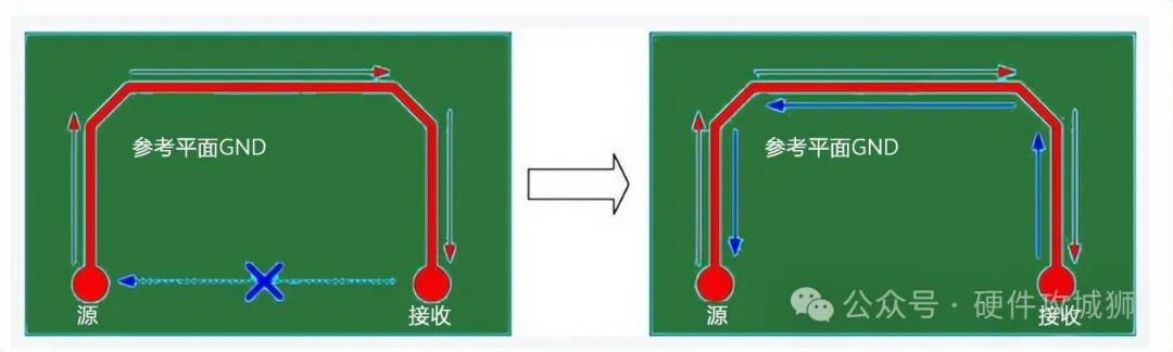
Return current path of high-speed signals
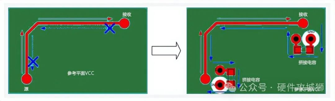
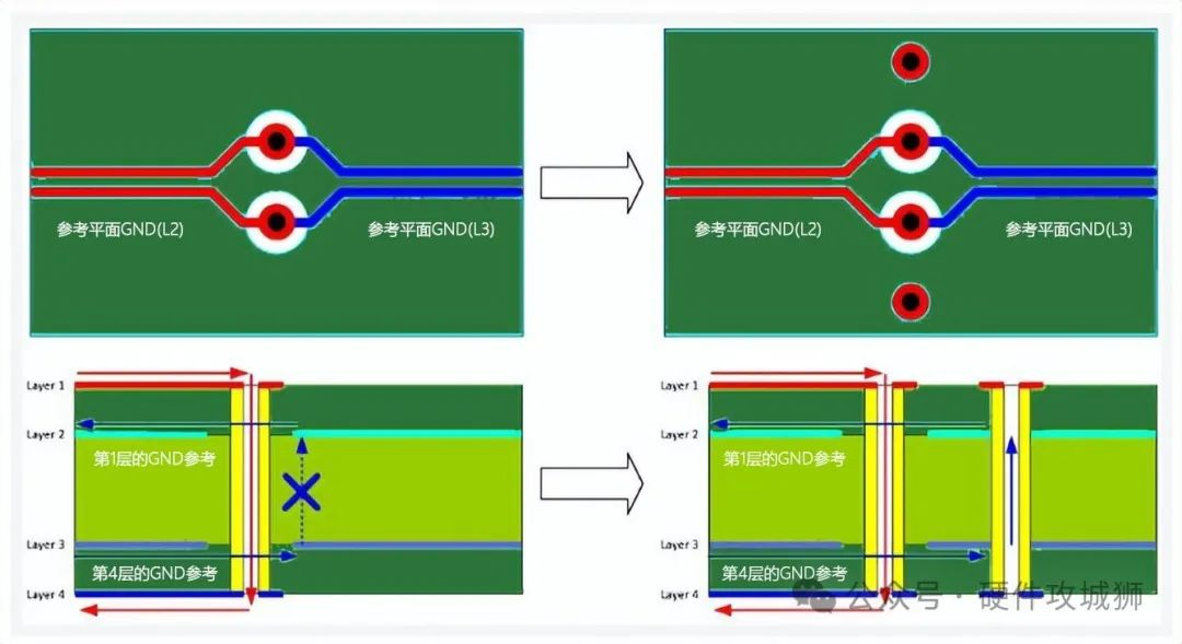
Never route signals over split planes, as the return path cannot follow the signal trace. If a plane is split between the receiver and source, the signal trace must be routed around the split; a separated forward and return path forms a loop antenna.
Prohibition of signal routing over split planes
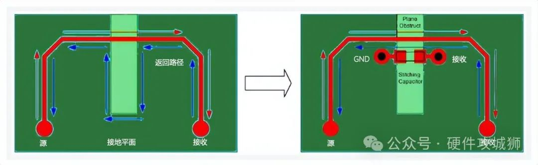
If signals must be routed across two different reference planes, add stitch capacitors to allow return current to transfer between planes. Place stitch capacitors close to the signal path to minimize the distance between the forward and return paths; the typical value of stitch capacitors is 10nF to 100nF.
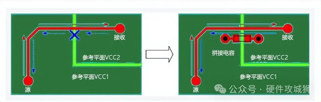
Stitch capacitor placement over split planes
Avoid plane obstacles and slots whenever possible. If routing around such obstacles is necessary, use stitch capacitors.
Stitch capacitor placement around plane obstacles
Designers should be cautious of voids in reference planes when routing high-speed signals. Voids form when vias are placed too close together; avoid large voids by ensuring sufficient spacing between vias, and minimize the number of ground/power vias to reduce via clearance requirements.
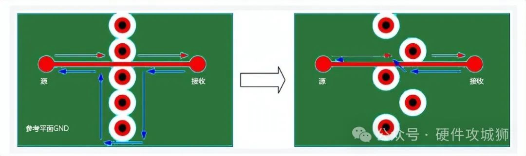
Avoiding voids in reference planes caused by dense vias
Return paths exist at the signal source and receiver. A single ground via at the source side (poor design) prevents return current from returning to the reference ground plane, forcing the return path onto the top-layer ground trace—while the signal trace impedance is calculated based on the ground plane, not the top-layer ground trace. Always place ground vias at both the source and receiver to allow return current to the ground plane.
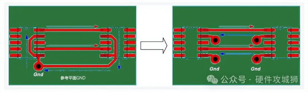
Ground via placement for proper return paths (Poor design on the left; Optimal design on the right)
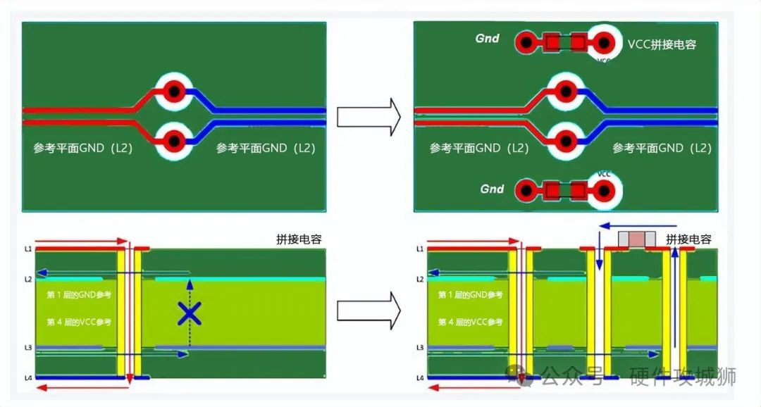
When a power plane is used as the signal reference, the signal return current should flow through the power plane (with the signal referenced to ground at the source and receiver). To switch the reference to the power layer, add stitch capacitors at the sink and source. If the receiver and source share the same power rail, bypass capacitors can serve as stitch capacitors when placed close to the signal start/exit points (ideal value: 10nF to 100nF).
Stitch capacitor usage when using a power plane as the reference
When differential signals switch layers, the reference ground plane also switches. Add stitch vias near the layer-changing vias to allow return current to switch ground layers; stitch vias must be placed symmetrically for differential signals.
Stitch via placement for differential signals switching ground layers
When signals switch to a different layer with a different reference plane, implement stitch capacitors to allow return current to flow from ground to the power layer; place and route stitch capacitors symmetrically for differential pairs.
Stitch capacitor placement for signals switching reference planes
Do not route high-speed signals at the edge of reference planes or near PCB boundaries, as this adversely affects trace impedance.
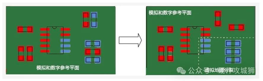
9. Separate Analog and Digital Ground Planes to Reduce Noise
Define separate analog and digital ground sections in the schematic to clearly identify which components/pins connect to digital ground and which to analog ground. This design is implemented by routing with two distinct ground planes as references, placed such that digital and analog components are located below their corresponding ground sections.
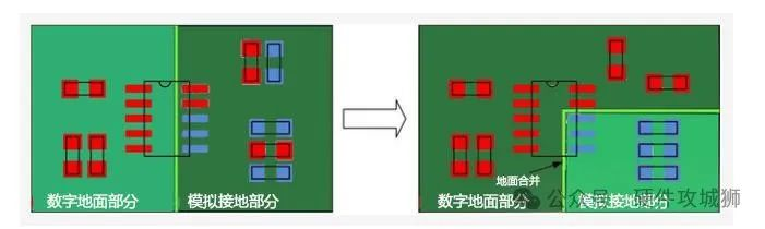
Separation of analog and digital ground planes
Exercise caution when splitting power planes.
Mixed-signal circuits require single-point connection of analog and digital ground planes. In the schematic, place a ferrite bead or 0Ω resistor between the analog and digital sections, and merge the two grounds close to the integrated circuit. In mixed-signal designs with split planes:
- Do not route digital signals over the analog ground plane
- Do not route analog signals over the digital ground plane
Prohibition of cross-plane signal routing
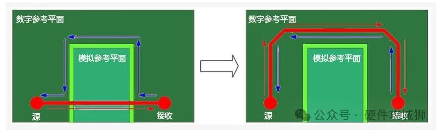
10. Use a Virtual Divider for Analog and Digital Ground Layout
In a virtual division, analog and digital grounds are not separated in the schematic or electrically in the layout—instead, an imaginary divider line is drawn between them in the physical layout. Components must be placed on the correct side of the virtual divider, and the divider line should have a simple shape (no plane obstacles to separate analog/digital return currents).
Virtual divider for analog and digital reference planes
Digital and analog signal traces must not cross the virtual divider line.
11. Match Component Pad Width to Trace Width for Optimal High-Speed Performance
PCB design starts with the schematic, especially component selection—SMD components are preferred because their smaller size and shorter leads provide more stable high-speed performance.
Optimal high-speed performance is achieved when the component pad width is close to the trace width, which helps reduce impedance matching issues between traces and component pads.
Trace width matching for different component packages
About Maxipcb
Maxipcb empowers innovators to turn cutting-edge technologies into reality.
We offer one-stop solutions for design, simulation, testing, PCB manufacturing, component procurement and SMT assembly, enabling efficient development, rapid deployment and risk control across the full product lifecycle.Serving the world in communications, industrial automation, aerospace, automotive, semiconductor and beyond, we build a safer, more connected future together.


