When designing a PCB, if there is a large current, it is necessary to design the corresponding line widths for different current values. In the past, the advice given by the master was that the line width of 1mm exceeded the current of 1A, and it can be estimated according to this.
When designing a PCB, if there is a large current, it is necessary to design the corresponding line widths for different current values. In the past, the advice given by the master was that the line width of 1mm exceeded the current of 1A, and it can be estimated according to this.
However, this method will still bring a lot of troubles in the actual design. For example, due to the structure and area limitation of the board, the board area of some products is not sufficient. If you take a line width of 0.5mm, it will not work if the current exceeds 1A. If not, what will be the problem? If the line width cannot be widened, is there any other way to improve the overcurrent capability?
Let's take a look at the more specific design, as shown in the following table, which is the optional PCB parameter options for Jialichuang PCB.

Seeing the above PCB parameters, there are more problems.
1. Is the line width design rule of the inner copper thickness consistent with the outer copper thickness?
2. Does the thickness of finished product have any effect on overcurrent?
3. What is the difference between copper thickness of 1 ounce and 2 ounces?
Let's look at the first question first. If the inner copper thickness and the outer copper thickness pass the same current, for example, 1A, are the line widths designed the same?
Before 2009, before the IPC-2152 standard was released, the PCB design adopted IPC-2221 (generic standard on printed board design).
This standard has three important reference figures as follows:
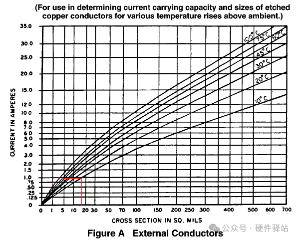
The figure below shows the cross-sectional area and overcurrent comparison table of the outer copper.
The red mark is the comparison of overcurrent and cross-sectional area for 1 year at a temperature of 10℃.
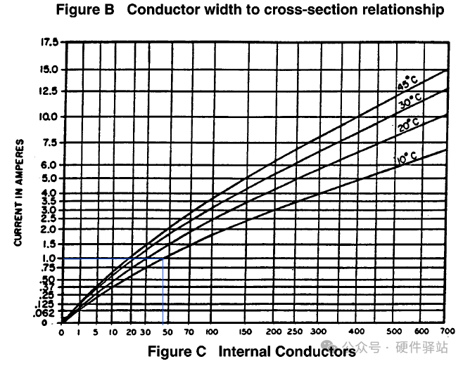
The following figure is the cross-sectional area and overcurrent comparison table of inner copper.
The blue mark is the comparison of overcurrent and cross-sectional area of 1A when the temperature rises to 10℃.
What we need to design PCB is line width, so the cross-sectional area needs to be further converted into line width, which can be found with reference to the following figure.
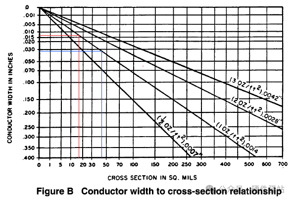
From the above graphical look-up table, the results are as follows:
According to IPC-2221 standard, the overcurrent of 1A and the copper thickness of 1OZ are evaluated according to the temperature rise of 10℃.
The line width of the outer trace is about 13mils(0.33mm).
The line width of the inner trace is about 32mils(0.81mm).
The calculation formula is also given in the standard. Under the same conditions, the K value of the inner layer is halved relative to the outer layer (that is, the current is reduced by half).
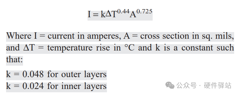
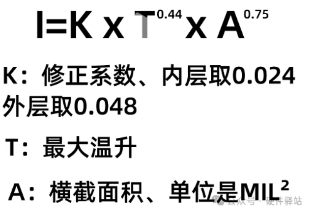
According to the above analysis, the conclusion of the first question seems to have been reached, that is, the line width design of the inner layer is wider than that of the outer layer for the same overcurrent design.
However, the above conclusion is wrong.
The data of this standard has not been verified by time, but simply reduces the internal conductor overcurrent data by half. For example, for the same line width, the designed overcurrent of the outer layer is 1A, then the same line width and the overcurrent of the inner layer are calculated as 0.5A. The assumption is that the internal wiring of PCB is not as fast as the external wiring. Of course, according to this method, except for wasting some copper skin, it will not bring other problems to the electrical characteristics of the product.
Later, after research, it was found that there was not much difference between the wiring heat dissipation in the inner layer of PCB and that in the outer layer. The new standard is IPC 2152 (standard for determining current carrying capacity in printed board design). This standard was issued in 2009.
As shown below, the new standard, inner layer and outer layer are unified into one chart.
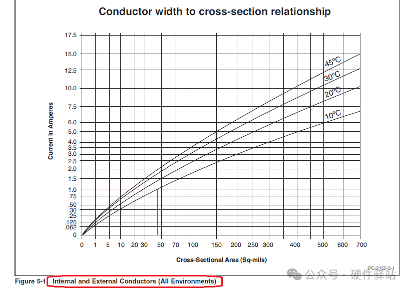
Going back to the second question, does the thickness of finished products have any influence on the design rules of line width? The answer is yes.
The standards are explained as follows: the thinner the thickness, the worse the heat dissipation, so the same current needs to be designed with a wider line width.

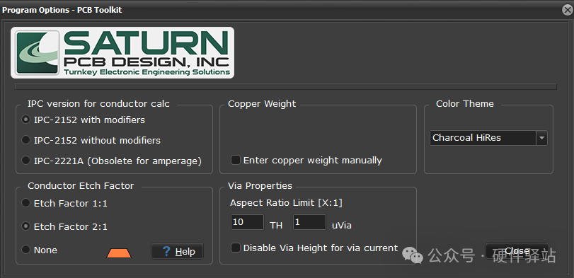
The IPC2152 standard gives many graphs, which can be used for reference. This method is too inefficient. You can use software to design the line width. "Saturn_PCB_Toolkit" is a very practical software. For the download link, please refer to the article:
Open the software and select the standard: "IPC-2152 with modifiers".
Select "Conductor Properties", set various parameters, and then you can calculate.
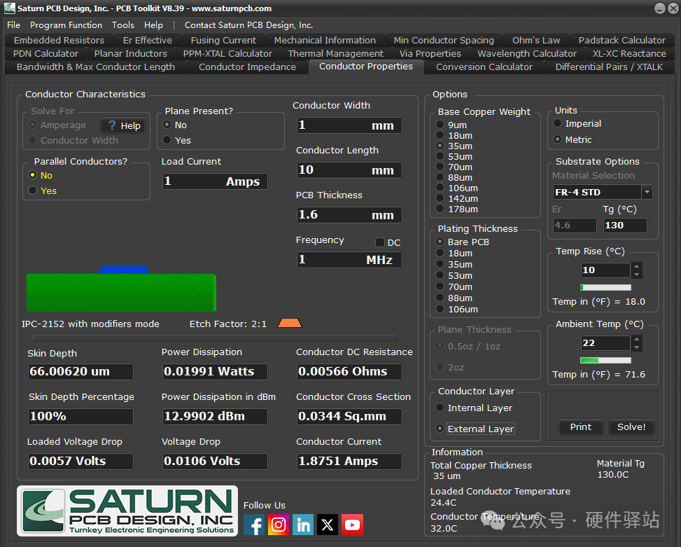
The plate thickness of 1.6mm, the copper thickness of 0.5OZ, 1OZ and 2OZ were compared respectively, and the temperature rose by 10℃, and the currents corresponding to different line widths were calculated. At the same time, a list of comparative data of 1mm thickness is added as follows:
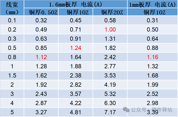
According to the calculation results of the above data, the most common thickness is 1.6mm, and the copper thickness is 1OZ. Under the condition that a current is required, the line width design of 0.5mm can meet the design requirements.
Besides board thickness, copper thickness, line width and temperature rise, PCB board, adjacent wires in the same layer, adjacent copper plane, surface coating, etching factor and other factors will all affect the overcurrent capacity. Interested parties can try to modify the relevant parameters for verification.
Summary:1. The overcurrent capability of inner and outer traces with the same width and copper thickness is not 2 times different. 2. It is a relatively conservative design to design a line width of 1mm to pass a current of 1A, and the design margin is large enough. 3. Sometimes what Mammy Yung says is not necessarily right.
About Maxipcb
Maxipcb empowers innovators to turn cutting-edge technologies into reality.
We offer one-stop solutions for design, simulation, testing, PCB manufacturing, component procurement and SMT assembly, enabling efficient development, rapid deployment and risk control across the full product lifecycle.
Serving the world in communications, industrial automation, aerospace, automotive, semiconductor and beyond, we build a safer, more connected future together.

