Today, we will give you a brief introduction to PCB teardrops, mainly covering: What is a PCB teardrop? What are the types of PCB teardrops? What are the functions of PCB teardrops? How to design PCB teardrops? How to design PCB teardrop pads?
Today, we will give you a brief introduction to PCB teardrops, mainly covering: What is a PCB teardrop? What are the types of PCB teardrops? What are the functions of PCB teardrops? How to design PCB teardrops? How to design PCB teardrop pads?
1. What is a PCB Teardrop?
A teardrop is additional copper, either straight or curved, placed at the junction between a pad or via and a trace, or at the transition where a trace changes between different widths. For example, if the width of part of your trace changes from 10 mil to 4 mil, a teardrop is added at the transition point to reduce any stress or fine line cracking.
Adding teardrops during the design process is a method to prevent drill breakout, as it slightly increases the amount of copper outside the pad. If the drill is offset to the opposite side of the trace, there is no issue as the connection on the trace remains intact. However, if the drill is offset to the junction between the trace and the pad, it may lead to serious long-term reliability problems.
In normal use, teardrops appear as small triangular fillets between the trace and the pad, and may also support other shapes such as concave or snowman styles, as shown in the figure below.
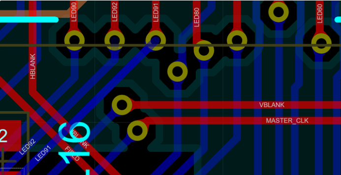
Teardrops Applied to Trace Connections
2. What are the Types of PCB Teardrops?
One method, known as the "snowman" style, involves adding an auxiliary pad at the junction between the existing pad and the trace. The auxiliary pad is smaller than the main pad, with its center positioned a few mils away from the center of the main pad, as shown in the middle figure below.
Another more common method, known as the curved or straight style, adds multiple traces from the existing pad to the existing trace, as shown in the left figure below.
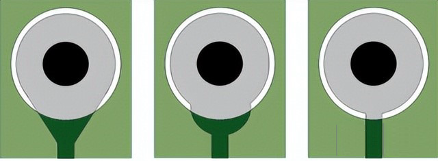
Teardrop Style Diagram
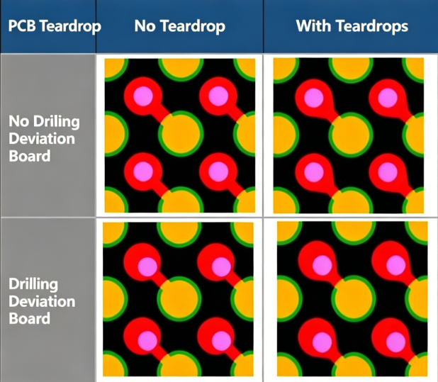
PCB Teardrop Comparison Diagram
3. What are the Functions of PCB Teardrops?
1. Reduce Drill Breakout and Improve Manufacturing Yield
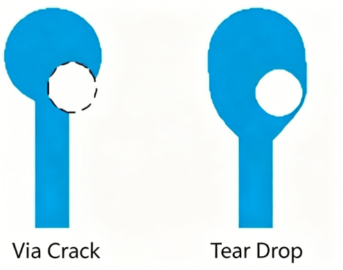
Functional Diagram of PCB Teardrops
Although manufacturers aim to produce high-quality PCBs during fabrication, drill drift or layer shift within the board is prone to occur during the lamination process. If this happens, the drill may create a hole outside the pad or via, breaking the electrical connection, which is also known as breakout.
Adding teardrops during manufacturing is a method to prevent drill breakout, as it increases the amount of copper at the connection. If the breakout point is on the back side of the pad or via, away from the trace, the connection remains intact with no adverse effects. However, if the drill drifts toward the trace, the teardrop provides sufficient copper thickness to ensure the connection is not broken.
Teardrops help improve drilling tolerance, enhance connection reliability, and contribute to higher production yield.
2. Prevent Acid Traps and Improve Reliability
Alkaline and other chemicals used to remove photoresist and unwanted copper are highly corrosive. If they are not washed away during the etching and plating process, they will erode the copper traces and damage the connections. Narrow gaps and sharp angles in traces and routing are notoriously difficult to clean, and are known as acid traps.
Teardrops eliminate sharp acute angles, making them ideal for preventing acid traps in the design.
3. Reduce mechanical and thermal stress at the junction between the trace and the pad, thereby minimizing fine line cracking in the trace.
4. Expand the pad tolerance for PCB manufacturers. This simplifies the fabrication of the circuit board, reduces scrap boards during production, and in turn lowers the overall cost of complex circuit boards.
5. Reduce the risk of trace cracking.
6. Improve resistance to thermal shock, which mainly affects rework and wave soldering during the production process.
7. Enhance the thermal shock resistance of the product in harsh operating environments.
4. How to Design PCB Teardrops?
What is the appropriate thickness for teardrops? You can refer to the manufacturer's guidelines, which are usually provided. As a general rule of thumb, the following formula can be used:
Vertex Radius Factor = ((PAD Diameter - Hole Diameter)/1.8)
This is critical for via drilling where the ratio of trace width to pad diameter is small. For high-density military boards, the annular ring around the vias shall be retained.
Teardrops are added on flex-PCB layouts to reduce stress at the junction between traces and pads.
Teardrops are added under BGAs with a large number of vias, as shown in the figure below.
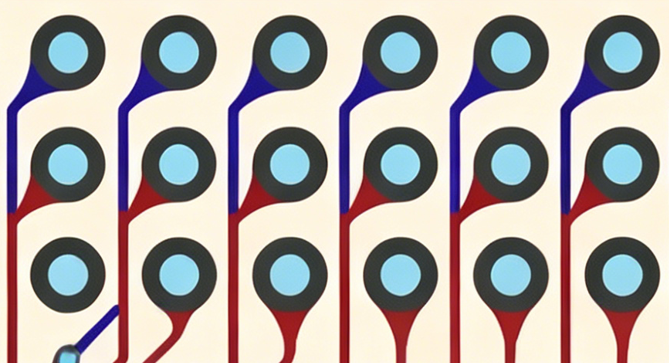
Teardrops Added Under BGA
Teardrops shall be added whenever a trace exits a pad, whether it is a solid pad or a pad with a via.
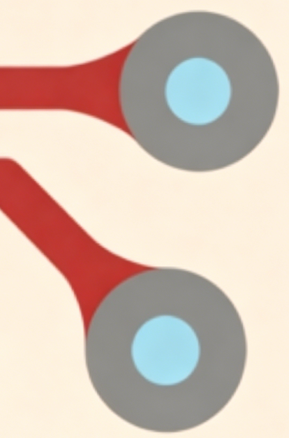
Teardrops Added to Pads
The importance of adding teardrops increases as the trace width becomes narrower.
Teardrops are not required for conductors wider than 20mil.
It is recommended to add teardrops to the PCB layout at the final stage of the design.
In some cases, this function is simply a checkbox in the CAD system, and teardrops can be added automatically with a single check.
For RF or high-frequency boards, teardrops shall be added during the design phase itself.
PCB manufacturers are equipped with a dedicated teardrop creation engine.
When the PCB manufacturer allows automatic teardrop creation, teardrop connections can be implemented while retaining the DFM routing.
5. How to Configure PCB Teardrops?
1. Configuring PCB Teardrops in Proteus
Teardrops are disabled by default in Proteus, but can be easily configured from the technical menu. Once enabled, teardrops are automatically added when trace connections are established, and recalculated and/or repositioned after trace editing. Teardrops are fully integrated with the design rule system and will not be generated where they would violate existing rules.
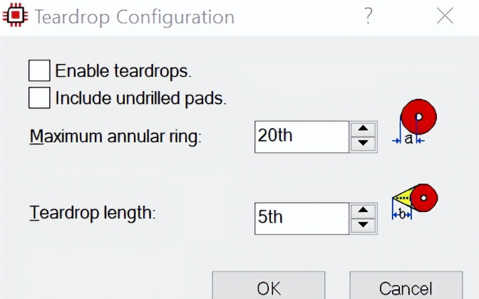
PCB Teardrop Configuration Interface
Once enabled, teardrops are updated globally across the board, so for complex designs, it is best to perform this operation at the late stage of the layout process. Edits to the teardrop configuration will also refresh the entire board, allowing you to include or exclude additional pads at a later stage.
2. Configuring PCB Teardrops in Altium Designer
You can simply specify the parameters of the teardrops, and quickly add or remove this copper feature through the dialog box (see Figure 1). The global nature and control of this function are extremely useful for fine-tuning PCB manufacturability.
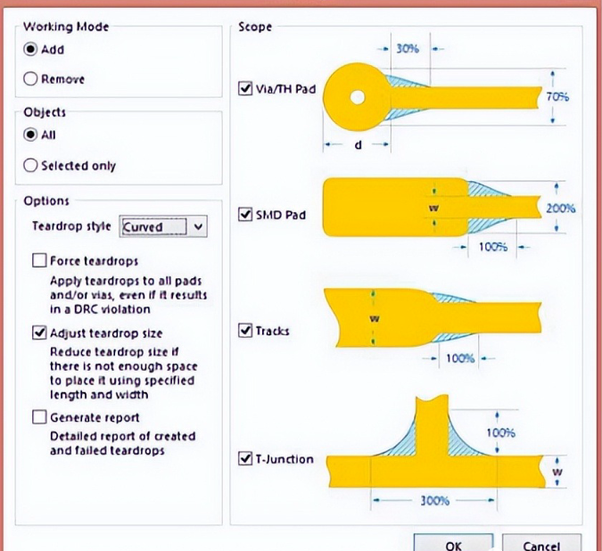
Teardrop Configuration Dialog Box in Altium Designer
The following two figures show teardrops applied to vias, through-hole pads, surface mount pads, traces, and T-junctions.
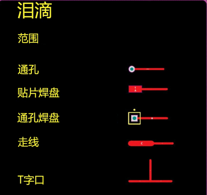
Teardrop Diagram Before Adding Teardrops
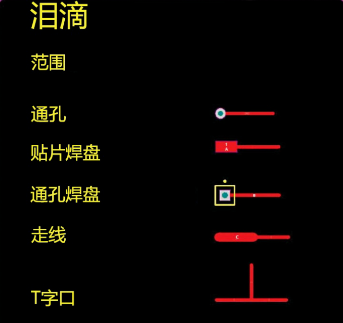
Teardrop Diagram After Adding Teardrops
Additional teardrop style modifications can be applied, as shown in the two figures below, which demonstrate the lined and curved teardrop styles respectively.
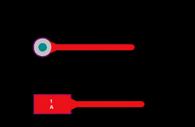
Lined Teardrop Style for Vias and Pads
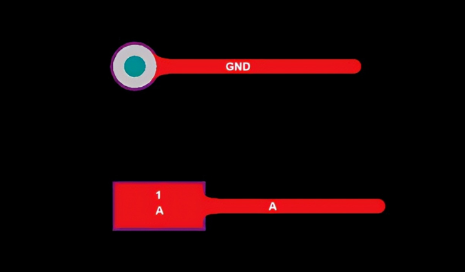
Curved Teardrop Style for Vias and Pads
3. Configuring PCB Teardrops in CAD
First, in the settings, there is an "Assignment" tab and an "Advanced Settings" tab. The "Advanced Settings" tab is used to configure the actual parameters, while the "Assignment" tab is used to configure which settings are assigned to which nets.
- Create a net class from the "Net Class" tab
- Configure the parameters in the "Advanced Settings" tab
- Assign the settings to the net class in the "Assignment" tab
The description of each setting tab is explained below:
Description of Setting Tabs
-
Teardrop Parameter Settings
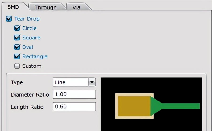
Teardrop Setting Interface
-
Object Settings
The objects applicable to the teardrop shape are "Pads", "SMDs" and "Vias".
PCB Teardrop Object Settings
- Teardrop Function Settings
Configure whether to apply the teardrop shape to the connection between the land and trace for each object, as well as the shape parameters.
Teardrop Function Settings
Only the teardrop configuration methods for 3 software are listed here. For specific details, you can go to the official website of the corresponding software, where corresponding tutorials are available.
About Maxipcb
Maxipcb empowers innovators to turn cutting-edge technologies into reality.
We offer one-stop solutions for design, simulation, testing, PCB manufacturing, component procurement and SMT assembly, enabling efficient development, rapid deployment and risk control across the full product lifecycle.Serving the world in communications, industrial automation, aerospace, automotive, semiconductor and beyond, we build a safer, more connected future together.


 Teardrops Applied to Trace Connections
 Teardrop Style Diagram
 PCB Teardrop Comparison Diagram
 Teardrops Added Under BGA
 Teardrops Added to Pads
 PCB Teardrop Configuration Interface
 Teardrop Configuration Dialog Box in Altium Designer
 Teardrop Diagram Before Adding Teardrops
 Lined Teardrop Style for Vias and Pads
 Curved Teardrop Style for Vias and Pads
 Teardrop Setting Interface
