PCB copper pour refers to the copper-filled area in a PCB layer. This layer can be the top, bottom, or any internal layer of the PCB stack-up, and PCB copper pour can be used for grounding, reference, or isolating specific components or circuits from other elements on the layer.
1. What is PCB Copper Pour?
PCB copper pour refers to the copper-filled area in a PCB layer. This layer can be the top, bottom, or any internal layer of the PCB stack-up, and PCB copper pour can be used for grounding, reference, or isolating specific components or circuits from other elements on the layer.
2. Copper Pour and Ground Copper Pour
- Copper Pour: A copper-filled area in a PCB layer; copper pour with through vias can be used to assist heat dissipation.
- Ground Plane: An internal layer in the circuit board stack-up, fully filled with copper, used as the ground or reference for signals or power supplies.
- Ground Copper Pour: Copper pour used for grounding that does not occupy the entire layer.
3. Functions of PCB Copper Pour
- Grounding on Double-Sided PCBs: Both layers of the board are used for signal routing without a dedicated ground plane. For these circuit boards, ground copper pour can significantly facilitate efficient routing by providing a central ground connection.
- EMI Shielding: For a well-designed multilayer board, a ground plane between two signal layers is required to minimize noise. If there is an internal signal layer adjacent to the surface signal layer, ground copper pour can help reduce noise by adding shielding.
- Heat Dissipation: Ground copper pour can also be used to draw heat away from high-power components, and thermal vias can then be used to remove excess heat from the circuit board.
- Copper Balance: PCB ground copper pour can also balance the copper volume on both sides of the circuit board during PCB assembly for the Contract Manufacturer (CM), reducing the possibility of warpage during reflow soldering. In this case, a cross copper grid may be a better alternative to solid copper ground pour.
- Large Current Path: Adding surface ground copper pour can provide a shorter return path for high-current devices, such as switching converters, instead of routing longer traces to the ground plane.
- Facilitation of PCB Manufacturing: Providing uniform copper distribution on a layer optimizes the etching and plating processes, and reduces the amount of etchant used in PCB manufacturing (thus lowering costs).
- RF and Microwave Design: Ground copper pour contains electromagnetic (EM) radiation in local areas, thereby reducing spurious coupling, radiation and dispersion.
- Digital Design: The ground plane improves noise immunity, achieves better grounding uniformity, and provides a low-inductance current path.
4. PCB Copper Pour Methods
When should copper pour be used? Generally, copper pour is used in scenarios requiring low resistance, low inductance, and heat dissipation. There are two basic methods for copper pour:
- Large-area solid copper pour
- Copper grid pour
A frequently asked question is whether large-area solid copper pour is better than copper grid pour. It is difficult to give a definitive answer.
- Large-area Solid Copper Pour
It provides the dual functions of current-carrying capacity enhancement and shielding. However, if wave soldering is adopted, it may cause board warpage and even blistering. In this case, several slots are usually cut to reduce blistering of the copper foil.
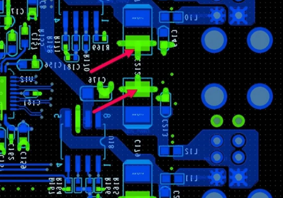
PCB Copper Pour
- Pure Copper Grid Pour
It mainly plays a shielding role, with a weakened effect on increasing current-carrying capacity and better heat dissipation performance. However, it should be noted that the copper grid is composed of staggered and widened traces. For circuits, the trace width has a corresponding "electrical length" related to the operating frequency of the circuit board. The actual electrical length can be obtained by dividing the digital frequency corresponding to the operating frequency, which can be found in relevant books.
When the operating frequency is not very high, the effect of the grid lines may not be obvious. Once the electrical length matches the operating frequency, serious problems will occur. You will find that the circuit cannot work properly at all, and the system is full of signals that interfere with its operation.
Therefore, for the use of grid pour, our recommendation is to select it according to the operating conditions of the designed circuit board, rather than sticking to one method blindly. For this reason, high-frequency circuits have high requirements for anti-interference performance using grid pour, and large-current circuits usually use solid copper pour to complete the auxiliary circuit.
5. Correct Methods for PCB Copper Pour
- Setting Up PCB Copper Pour in CAD Tools
Increase the isolation clearance to 8mil for 1oz copper, and to 10mil for 2oz copper in CAD tools.
- The default isolation clearance between the copper layer and signal traces is "6 mil".
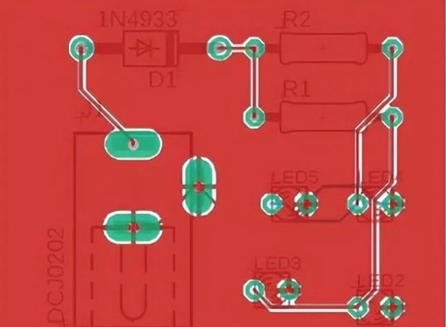
Correct Method for PCB Copper Pour
- To increase the clearance, right-click the edge of the polygon and go to Properties.
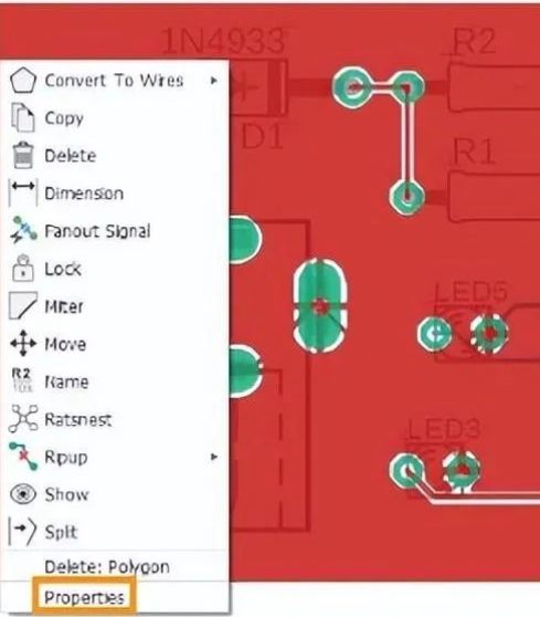
Correct Method for PCB Copper Pour
- In the Properties dialog box, change the isolation value to 10mil, click "Apply", and then click "OK".
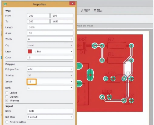
Correct Method for PCB Copper Pour
- The spacing between the copper layer and signal traces will be increased accordingly.
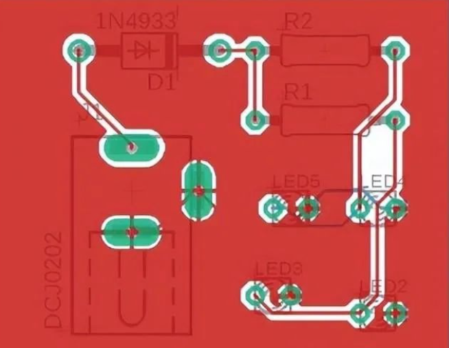
Correct Method for PCB Copper Pour
6. Copper Pour Area Design
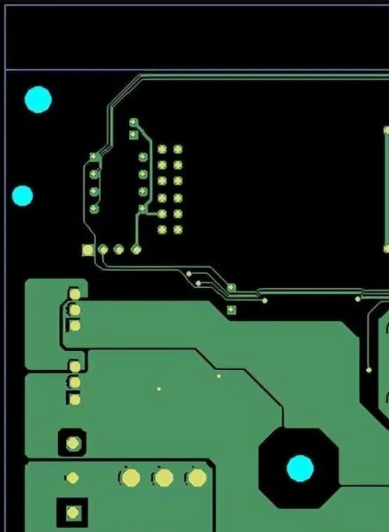
Copper Pour Area Design
7. Key Points for PCB Copper Pour
- Copper pour is sometimes used incorrectly merely to fill unused space on the circuit board.
- CAM engineers can add copper thief patterns to balance the copper distribution on the layer.
- Floating (unconnected copper) is a real hazard to signal integrity, and all copper pour must be grounded.
- Ground copper pour without ground vias may become a channel for crosstalk between traces on both sides of the ground shape.
- By creating the copper pour layer as part of the ground grid and configuring it as a solid plane, a well-defined return current path can be provided.
- Any additional planes must be properly positioned and spaced so that they do not adversely affect the signal integrity of the circuit board.
- Grounding on the microstrip layer changes the transmission line from a microstrip to a grounded coplanar waveguide (CPW).
- Copper pour can reduce the characteristic impedance and differential impedance of the transmission line.
- CPW confines electromagnetic fields in a more localized manner than microstrip lines, thereby reducing spurious coupling, radiation and dispersion.
- Microstrip lines can radiate, while striplines do not, as the fields are confined between the ground planes.
- When copper pour is placed close to critical signal traces, the impedance will be reduced by 2–3 ohms.
- Copper pour may convert differential mode signals to common mode signals at these points, thereby affecting signal integrity.
About Maxipcb
Maxipcb empowers innovators to turn cutting-edge technologies into reality.
We offer one-stop solutions for design, simulation, testing, PCB manufacturing, component procurement and SMT assembly, enabling efficient development, rapid deployment and risk control across the full product lifecycle.Serving the world in communications, industrial automation, aerospace, automotive, semiconductor and beyond, we build a safer, more connected future together.


 PCB Copper Pour
 Correct Method for PCB Copper Pour
 Correct Method for PCB Copper Pour
 Correct Method for PCB Copper Pour
 Correct Method for PCB Copper Pour
 Copper Pour Area Design
