Microwave transmission lines are the foundation of radio frequency (RF) systems. We provided a detailed summary of common microwave transmission lines in Summary of RF Transmission Lines. Today, we will introduce the most widely used microwave transmission line — microstrip line.
Microwave transmission lines are the foundation of radio frequency (RF) systems. We provided a detailed summary of common microwave transmission lines in Summary of RF Transmission Lines. Today, we will introduce the most widely used microwave transmission line — microstrip line.
History of Microstrip Line
As the most widely applied transmission line at present, the microstrip line has a history of more than 70 years. It was first proposed by Grieg and Engelmann from ITT Laboratories of the United States and presented as a new type of printed circuit at the IRE Conference in December 1952. Its main competitor is the stripline, which was invented by R. Barrett in the 1950s and is two years "older" than the microstrip line. The stripline was originally named Tri-plate, which is easy to understand as it consists of exactly three metal layers.
Although stripline and microstrip line are highly similar, they have different origins. In terms of evolutionary relationship, the microstrip line is one generation earlier than the stripline. The microstrip line can be regarded as an extension of the parallel two-wire transmission line, the oldest microwave transmission line. A metal conductive plate is placed on the central plane of the parallel two-wire line, perpendicular to all electric field lines, maintaining the original electromagnetic field structure. After removing one of the two wires, the electromagnetic field structure of the remaining wire remains unchanged. The remaining wire and the metal conductive plate form a new transmission line — the microstrip line. A metal strip is coated on one side of a dielectric board, and a metal ground plane is on the other side.
Evolution of Microstrip Line from Parallel Two-Wire Transmission Line
The stripline can be regarded as evolved from the coaxial cable. The outer conductor of the coaxial cable is split into two parts, flattened into a flat plate, and the inner conductor is also flattened into a strip, forming the stripline.
Evolution of Stripline from Coaxial CableThe coaxial cable was invented to solve the radiation loss problem of parallel two-wire lines. It can be regarded as formed by expanding one wire of the parallel two-wire line and wrapping the other wire. From this perspective, the coaxial cable is an intermediate structure between the stripline and the parallel two-wire line.
Illustration: Electric Field Distribution of Stripline and Microstrip LineBy observing the electric field distribution of stripline and microstrip line: if the metal ground plane is large enough, the electromagnetic field of the stripline is enclosed between two conductor plates with symmetrical upper and lower distribution, maintaining the purity and stability of the TEM mode. However, the microstrip line has obvious electromagnetic radiation in the open area, and its electromagnetic field distribution is significantly asymmetric. This asymmetric field structure caused considerable troubles in the early days of the microstrip line, including notable radiation loss and excitation of unwanted modes that degrade the operating mode. Therefore, this asymmetric operating mode is called the quasi-TEM mode.
These drawbacks can be improved by reducing the cross-sectional dimensions of the microstrip line — making the thickness of the dielectric substrate and the width of the conductor strip much smaller than the operating wavelength. However, this will introduce greater conductor loss. As a result, the microstrip line was at a significant disadvantage in competition with the stripline in the early stage and was not widely used.
With technological development, the application of multilayer PCBs has become increasingly popular, and microstrip lines and striplines are eventually integrated into the same circuit board.
In any case, the emergence of stripline and microstrip line has brought microwave transmission lines into the planar era. Printed circuit board technology has been widely used in RF circuits, enabling today's wireless era.
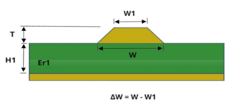
Structure of Microstrip Line
As mentioned above, the microstrip line consists of a dielectric substrate, a metal strip on the top surface of the substrate, and a metal ground plane on the bottom surface, as shown in the figure below. Therefore, research on the microstrip line focuses on these three components: metal strip, dielectric substrate, and ground plane, among which the dielectric substrate is the most critical.
Structural Diagram of Microstrip Line
The requirements for the dielectric substrate are the most stringent:
- High dielectric constant to meet the miniaturization requirements of circuits.
- Low loss, with a small loss tangent (tanδ) — the smaller, the better.
- Stable dielectric constant at least within the specified frequency and temperature ranges.
- High breakdown strength to enable the microstrip line to transmit higher power.
- High thermal conductivity to ensure efficient heat dissipation.
- Good adhesion to metal for convenient metal layer printing.
The following table (from Microstrip Circuits) compares dielectric substrate materials suitable for millimeter-wave applications. Different materials have different dielectric constants and loss factors. Alumina appears three times in the table; higher purity of alumina corresponds to a higher dielectric constant and lower loss.
Table 1-1 Properties of Substrate Materials
| Material |
Main Component |
Dielectric Constant |
tanδ (10GHz) |
Thermal Conductivity (W/cm·°C) |
Surface Roughness (μ) |
Machinability |
Chemical Resistance |
| Fused Silica |
SiO₂ (99.9%) |
3.8 |
10⁻⁴ |
0.01 |
<0.1 |
Good |
Good |
| 96% Alumina Ceramic |
Al₂O₃ (96%) |
8.9 |
6×10⁻⁴ |
0.35 |
<2 |
None |
Good |
| 99.6% Alumina |
Al₂O₃ (99.6%) |
9.5–9.6 |
2×10⁻⁴ |
0.4 |
<1 |
None |
Good |
| Sapphire |
Al₂O₃ (100%) |
11 |
10⁻⁴ |
0.4 |
<0.1 |
None |
Good |
| Beryllium Oxide |
BeO (95–99%) |
6 |
10⁻⁴ |
2.5 |
<0.2 |
Poor |
Good |
| Rutile |
TiO₂ |
100 |
4×10⁻⁴ |
0.02 |
<2 |
None |
Good |
| Glass |
— |
5 |
4×10⁻⁸ |
0.01 |
Good |
None |
Poor |
The following table compares common dielectric sheets. For more material comparisons, refer to the Rogers official website (Rogers High-Frequency Circuit Board Selection Guide).
Another key component of the microstrip line is the metal strip, which requires excellent electrical conductivity and strong adhesion to the dielectric board to ensure structural stability. Silver, copper, and gold have high conductivity but poor adhesion; molybdenum, chromium, and tantalum have good adhesion but low conductivity. The properties of these materials are listed in the following table (from Microstrip Circuits):
Table 1-2 Properties of Various Metal Materials
| Material |
Resistivity (Ω·cm) |
Skin Depth (2000MHz) |
Surface Resistivity (/cm²×10²) |
Thermal Expansion Coefficient (10⁻⁶/°C) |
Adhesion to Substrate |
| Silver |
1.59×10⁻⁶ |
1.4 |
2.5 |
21 |
Poor |
| Copper |
1.67×10⁻⁶ |
1.5 |
2.6 |
18 |
Very Poor |
| Gold |
2.35×10⁻⁶ |
1.7 |
3.0 |
15 |
Very Poor |
| Aluminum |
2.65×10⁻⁶ |
1.9 |
3.3 |
25 |
Very Poor |
| — |
5.34×10⁻⁶ |
2.6 |
4.7 |
4.6 |
Good |
| Molybdenum |
5.5×10⁻⁶ |
2.7 |
4.7 |
6.0 |
Good |
| Chromium |
12.7×10⁻⁶ |
2.7 |
4.7 |
9.0 |
Good |
| — |
15.2×10⁻⁶ |
4.0 |
7.2 |
6.6 |
Excellent |
For more material properties, refer to the article Material Encyclopedia.
In the fabrication of microstrip lines, a thin metal layer with good adhesion is first evaporated on the dielectric substrate. Its thickness is much smaller than the skin depth at the operating frequency of the microstrip line, usually only tens to hundreds of angstroms. Then a high-conductivity metal layer is deposited. Electromagnetic waves can completely penetrate this thin metal layer, with most energy distributed on the high-conductivity metal, minimizing the impact on microstrip line loss.
Impedance Calculation of Microstrip Line
Many software tools are available for microstrip line impedance calculation, such as AWR TxLine (send "txline" to get the download link). Interested readers can also input the following formulas into Excel for calculation.
Calculations can also be performed via the following link:
Loss of Microstrip Line
Loss is a critical parameter in RF design; for valuable RF signals, lower loss is better. The loss of microstrip lines is much higher than that of common waveguides and coaxial cables, so microstrip line loss requires special attention in circuit design. Microstrip line loss generally consists of three components: conductor loss, dielectric loss, and radiation loss.
- Conductor Loss: Loss caused by the conductor strip and ground plane of the microstrip line. Metal conductors have finite conductivity, resulting in resistive loss when current passes through. Conductor loss is the dominant part of microstrip line loss.
- Dielectric Loss: Thermal loss generated by alternating polarization of dielectric molecules and lattice collisions when electromagnetic waves pass through dielectric materials, usually expressed by the loss tangent (tanδ). A smaller loss tangent corresponds to lower dielectric loss.
- Radiation Loss: The field distribution of the microstrip line is semi-open, leading to partial energy radiation. Radiation loss can be reduced by shrinking the cross-section of the microstrip line. However, radiation is significant at discontinuities of the microstrip line, which may severely affect the electromagnetic interference (EMI) of the entire RF system. Therefore, metal shielding covers are usually installed on microstrip circuits to suppress radiation, reduce radiation loss, and avoid interference with other circuits.
In addition to the three common losses above, there is magnetic loss: magnetic loss may occur in circuits using magnetic materials such as ferrite or garnet as dielectrics. These materials cause increased magnetic loss near their natural resonant frequency. The magnetic loss tangent and characteristic impedance rise rapidly at the resonant frequency, leading to increased magnetic loss. Conductor loss depends on characteristic impedance; as characteristic impedance increases at the resonant frequency, conductor loss increases with magnetic loss.
In an article from Microwave101, the author conducted a detailed comparative study on the loss of alumina (Al₂O₃) microstrip lines with different thicknesses. The conclusions are as follows:
- For alumina substrates of different thicknesses, dielectric loss is nearly unchanged, but thinner substrates result in higher metal loss. For the same impedance, a thinner dielectric substrate requires a narrower conductor strip of the microstrip line, leading to more concentrated current distribution and higher corresponding conductor loss.
Alumina Substrate, H=254 μm (10 mils), W=247 μm, εr=9.9, tanδ=0.0002, 3μm Gold, Conductivity=3.5×10⁷ S/m
| Frequency (GHz) |
tanδ Loss (dB/cm) |
Metal Loss (dB/cm) |
Total Loss (dB/cm) |
| 0 |
— |
-0.033 |
-0.033 |
| 10 |
-0.005 |
-0.119 |
-0.124 |
| 20 |
-0.009 |
-0.175 |
-0.184 |
| 30 |
-0.014 |
-0.217 |
-0.231 |
| 40 |
-0.019 |
-0.249 |
-0.268 |
Alumina Substrate, H=127 μm (5 mils), W=120 μm, εr=9.9, tanδ=0.0002, 3μm Gold, Conductivity=3.5×10⁷ S/m
| Frequency (GHz) |
tanδ Loss (dB/cm) |
Metal Loss (dB/cm) |
Total Loss (dB/cm) |
| 0 |
— |
-0.069 |
-0.069 |
| 10 |
-0.004 |
-0.227 |
-0.231 |
| 20 |
-0.009 |
-0.333 |
-0.342 |
| 30 |
-0.013 |
-0.415 |
-0.429 |
| 40 |
-0.018 |
-0.483 |
-0.501 |
- Fused silica substrates have lower loss. Firstly, the loss tangent of fused silica is as low as 0.0001; secondly, its low dielectric constant allows a wider conductor strip of the microstrip line, resulting in lower metal loss.
Fused Silica Substrate, H=254 μm (10 mils), W=540 μm, εr=3.8, tanδ=0.0001, 3μm Gold, Conductivity=3.5×10⁷ S/m
| Frequency (GHz) |
tanδ Loss (dB/cm) |
Metal Loss (dB/cm) |
Total Loss (dB/cm) |
| 0 |
0 |
-0.015 |
-0.015 |
| 10 |
-0.001 |
-0.061 |
-0.063 |
| 20 |
-0.003 |
-0.091 |
-0.094 |
| 30 |
-0.004 |
-0.114 |
-0.118 |
| 40 |
-0.005 |
-0.132 |
-0.138 |
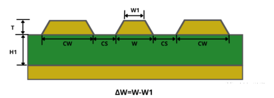
Microstrip Line Routing
-
Standard Microstrip Line
-
Differential Microstrip Line
-
- Coplanar Microstrip Line
About MaxipcbMaxipcb enables advanced electronic innovation. We deliver one-stop solutions including circuit design, simulation, testing, PCB fabrication, component sourcing and SMT&PCBA assembly, to boost R&D efficiency, speed up mass production and control full-cycle risks. We serve global sectors like communication, industrial automation, aerospace, automotive and semiconductor, jointly forging a safer, connected intelligent future.


