This article analyzes ESD failures caused by software design and PCB loop design, based on two real engineering cases.
This article analyzes ESD failures caused by software design and PCB loop design, based on two real engineering cases.
Case 1: Ambient Temperature Controller Black Screen During ±15kV Contact Discharge
1. Problem Description
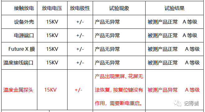
An intelligent ambient temperature controller for livestock houses was tested per GB/T 17626.2 with ±15kV contact discharge.
- When discharging on the metal temperature probe housing:
Display blackout, screen distortion, no auto-recovery; reset button invalid; only power cycle recovers.
- All other test points (enclosure, power port, cable, terminal) passed Grade A.
2. Product Principle
- Metal probe housing → connected to EARTH (PE ground)
- Internal thermistor → signal acquisition → AD conversion → main chip
- Temperature circuit uses single-point grounding; system GND is isolated from PE (floating system)
3. Analysis & Verification
3.1 Interference Path Identification
- Disconnect thermistor circuit; only keep probe housing connected to EARTH.
- ESD still causes blackout → interference is NOT from signal lines.
- Probe housing connects directly to PE; discharge should discharge to ground quickly.
- Conclusion: ESD couples into the system via radiation (electric/magnetic field), not conduction.
3.2 Magnetic Field Coupling Mechanism
ESD current generates strong magnetic fields.
- Larger loop area = stronger coupling
- Power and high-speed loops are usually controlled, but control signal loops are often ignored.
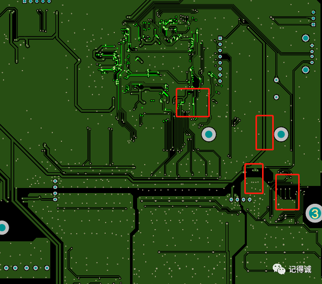
3.3 PCB Layout Defect
The PCB had severely split ground planes and poor grounding between modules, causing:
- Uncontrolled signal return paths
- Excessively large signal loops
- MCU disrupted → display failure
3.4 Improvement Test: Reduce Signal Loop Area
- Restore continuous reference ground under the temperature-sampling trace.
- Use copper tape to reconnect split ground planes below the signal path.
Ground plane restoration using copper tape (red box)
Result: After fixing ground continuity, ESD no longer causes black screen.
About Maxipcb
Maxipcb empowers innovators to turn cutting-edge technologies into reality.
We offer one-stop solutions for design, simulation, testing, PCB manufacturing, component procurement and SMT assembly, enabling efficient development, rapid deployment and risk control across the full product lifecycle.Serving the world in communications, industrial automation, aerospace, automotive, semiconductor and beyond, we build a safer, more connected future together.