In PCB design, the pad is a critical concept that must be familiar to every PCB engineer. However, despite their familiarity with pads, many engineers only have a superficial understanding of the professional knowledge related to pads.
In PCB design, the pad is a critical concept that must be familiar to every PCB engineer. However, despite their familiarity with pads, many engineers only have a superficial understanding of the professional knowledge related to pads.
Today, Circuit Jun will walk you through the types of pads, as well as the design standards for pads in PCB design.
A pad is the basic structural unit for surface mount assembly, used to form the land pattern of a printed circuit board, that is, various pad combinations designed for specific component types.
A pad is a partial conductive pattern used for electrical connection, component mounting, or both.
Types of PCB Pads
1. Common Pads
- Square Pads – Mostly adopted on printed boards with large, low-quantity components and simple printed traces. This type of pad is easy to implement in manual homemade PCB fabrication.
- Circular Pads – Widely used in single-sided and double-sided printed boards with regularly arranged components. If the board density permits, the pad can be designed with a larger size to prevent peeling off during soldering.
- Island Pads – The connecting traces between adjacent pads are integrated into a single body. They are commonly used in vertical irregular arrangement and mounting applications.
- Polygonal Pads – Used to distinguish pads with similar outer diameters but different hole diameters, facilitating machining and assembly.
- Oblong (Oval) Pads – This type of pad has a sufficient area to enhance peel resistance, and is commonly applied for dual in-line devices.
- Slotted (Open) Pads – Commonly used to ensure that the pad holes for manual repair soldering are not sealed by solder after wave soldering.
2. Special Pads
- Plum Blossom Pads
Plum blossom pads are usually used at the position of large vias for grounding. This design is adopted for the following reasons:
- The mounting hole needs to be metalized and connected to GND. If the mounting hole is fully metalized, it is easily blocked during reflow soldering.
- The use of internal metal screw holes may result in poor grounding status due to installation or repeated disassembly and assembly. The plum blossom pad design can ensure reliable grounding regardless of stress changes.
- Thermal Relief Pads
Thermal relief pads, also known as hot pads or thermal pads, are designed to reduce heat dissipation from the pad during soldering, so as to prevent cold solder joints or PCB delamination caused by excessive heat dissipation.
- When the pad is connected to the ground plane, the thermal relief design can reduce the area connected to the ground plane, slow down the heat dissipation rate, and facilitate soldering operations.
- For PCBs that require machine mounting and reflow soldering, thermal relief pads can prevent PCB delamination (as more heat is required to melt the solder paste).
- Teardrop Pads
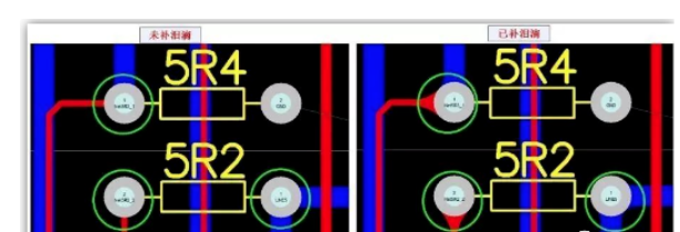 Teardrop pads are often used when the trace connected to the pad is thin, to prevent pad peeling or disconnection between the trace and the pad. This type of pad is widely used in high-frequency circuits.
Design Standards for Pads in PCB Design
1. Design Standards for the Shape and Size of PCB Pads
- Call the standard PCB footprint library for design.
- The minimum single-side size of the pad shall not be less than 0.25mm, and the maximum overall diameter of the pad shall not exceed 3 times the component hole diameter.
- Try to ensure that the spacing between the edges of two adjacent pads is greater than 0.4mm.
- For pads with a hole diameter exceeding 1.2mm or a pad diameter exceeding 3.0mm, they shall be designed as diamond-shaped or plum blossom pads.
- For high-density routing scenarios, oblong and long circular connection pads are recommended. The diameter or minimum width of pads on single-sided boards is 1.6mm; for pads of weak current circuits on double-sided boards, the hole diameter plus 0.5mm is sufficient. Excessively large pads are likely to cause unnecessary solder bridging.
2. Standard for Via Size of PCB Pads
The inner hole of the pad is generally not less than 0.6mm, because holes smaller than 0.6mm are difficult to process during die opening and punching. Usually, the diameter of the metal pin plus 0.2mm is taken as the inner hole diameter of the pad. For example, when the metal pin diameter of a resistor is 0.5mm, the corresponding inner hole diameter of its pad is 0.7mm, and the pad diameter is determined by the inner hole diameter.
3. Key Points for Reliability Design of PCB Pads
- Symmetry: To ensure the balance of surface tension of molten solder, the pads at both ends of the component must be symmetrical.
- Pad spacing: Excessively large or too small pad spacing will cause soldering defects, so it is necessary to ensure the appropriate spacing between the component ends or pins and the matching pads.
- Remaining size of the pad: The remaining size after the lap joint between the component end or pin and the pad must ensure that the solder joint can form a standard meniscus.
- Pad width: It shall be basically consistent with the width of the component end or pin.
About Maxipcb
Maxipcb empowers innovators to turn cutting-edge technologies into reality.
We offer one-stop solutions for design, simulation, testing, PCB manufacturing, component procurement and SMT assembly, enabling efficient development, rapid deployment and risk control across the full product lifecycle.Serving the world in communications, industrial automation, aerospace, automotive, semiconductor and beyond, we build a safer, more connected future together.

 Teardrop pads are often used when the trace connected to the pad is thin, to prevent pad peeling or disconnection between the trace and the pad. This type of pad is widely used in high-frequency circuits.