As energy conversion devices operating in switching mode, switching power supplies have high voltage and current change rates, resulting in strong interference. The main interference sources are concentrated in power switching devices, as well as associated heat sinks and high-frequency transformers—their positions are relatively clear compared to interference sources in digital circuits.
As energy conversion devices operating in switching mode, switching power supplies have high voltage and current change rates, resulting in strong interference. The main interference sources are concentrated in power switching devices, as well as associated heat sinks and high-frequency transformers—their positions are relatively clear compared to interference sources in digital circuits.
The switching frequency ranges from tens of kilohertz to several megahertz, with the main interference forms being conducted interference and near-field interference. PCB routing for switching power supplies is usually done manually, which is more arbitrary, increasing the difficulty of extracting PCB distributed parameters and estimating near-field interference.
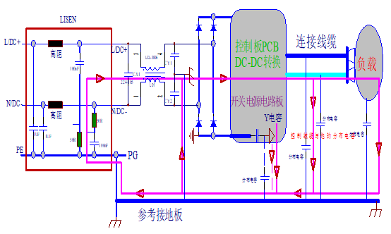 Switching power supply system interference diagram (High-impedance DC+, DC-DC Conversion, Control Board PCB, Connection Cable, Load, Y Capacitor, PE (Protective Earth), PG (Power Good), Reference Ground Plate, Distributed Capacitance Between Control Board and Ground)
I. 8 Interference Prevention Techniques by Frequency Band
- Below 1MHz: Dominated by differential-mode interference; increasing the X capacitor can resolve the issue.
- 1MHz ~ 5MHz: Mixed differential-mode and common-mode interference. Connect a series of X capacitors at the input end to filter out differential-mode interference, then identify and address the overstandard interference type.
- 5MHz ~ 10MHz: Dominated by common-mode interference; adopt common-mode suppression methods.
- 10MHz ~ 25MHz: For devices with earthed enclosures, winding the ground wire around a ferrite core twice can significantly attenuate interference above 10MHz.
- 25MHz ~ 30MHz: Measures include increasing the Y capacitor to ground, wrapping the transformer with copper tape, optimizing PCB layout, connecting a small bifilar-wound ferrite core (at least 10 turns) in front of the output line, and paralleling an RC filter across the output rectifier diode.
- 30MHz ~ 50MHz: Typically caused by the high-speed switching of MOSFETs. Solutions include increasing the MOS drive resistance, using slow diodes in the RCD snubber circuit, and adopting slow diodes for the VCC supply voltage.
- 100MHz ~ 200MHz (Case 1): Generally caused by the reverse recovery current of output rectifier diodes; series ferrite beads with rectifier diodes can mitigate the issue.
- 100MHz ~ 200MHz (Case 2): Mostly originating from PFC MOSFETs and PFC diodes. Series ferrite beads with MOSFETs and PFC diodes are effective and can basically solve the problem in the horizontal direction, but have limited effect in the vertical direction.
Note: The radiation from switching power supplies generally only affects frequency bands below 100MHz. Corresponding absorption circuits can also be added to MOSFETs and diodes, but this will slightly reduce efficiency.
II. EMI Prevention Measures in Switching Power Supply Design
- Minimize the PCB copper area of noise circuit nodes as much as possible, such as the drain and collector of switching tubes, and the nodes of primary and secondary windings.
- Keep input and output terminals away from noise-generating components, such as transformer windings, transformer cores, and heat sinks of switching tubes.
- Keep noise-generating components (e.g., unshielded transformer windings, unshielded transformer cores, switching tubes) away from enclosure edges—enclosure edges are likely to be close to external ground wires during normal operation.
- If the transformer is not equipped with electric field shielding, keep the shield and heat sink away from the transformer.
- Minimize the area of the following current loops: secondary (output) rectifiers, primary switching power devices, gate (base) drive circuits, and auxiliary rectifiers.
- Do not mix the gate (base) drive feedback loop with the primary switching circuit or auxiliary rectifier circuit.
- Adjust and optimize the damping resistance value to prevent ringing during the switch dead time.
- Prevent saturation of EMI filter inductors.
- Keep corner nodes and secondary circuit components away from the shield of the primary circuit or the heat sink of the switching tube.
- Keep oscillating nodes and component bodies of the primary circuit away from shields or heat sinks.
- Install high-frequency input EMI filters close to input cables or connectors.
- Install high-frequency output EMI filters close to output wire terminals.
- Maintain a certain distance between the PCB copper foil opposite the EMI filter and component bodies.
- Add resistors to the wiring of the auxiliary coil rectifier.
- Parallel a damping resistor across the ferrite rod coil.
- Parallel a damping resistor across the output RF filter.
- During PCB design, reserve space for a 1nF/500V ceramic capacitor or a series of resistors connected between the static end of the transformer primary and the auxiliary winding.
- Keep EMI filters away from power transformers, especially avoiding placement at the ends of windings.
- If PCB area permits, reserve pins for shielding windings and positions for RC dampers on the PCB—RC dampers can be connected across the shielding windings.
- If space allows, install a small radial lead capacitor (Miller capacitor, 10pF/1kV) between the drain and gate of the switching power MOSFET.
- If space permits, install a small RC damper at the DC output end.
- Do not place the AC socket close to the heat sink of the primary switching tube.

 Switching power supply system interference diagram (High-impedance DC+, DC-DC Conversion, Control Board PCB, Connection Cable, Load, Y Capacitor, PE (Protective Earth), PG (Power Good), Reference Ground Plate, Distributed Capacitance Between Control Board and Ground)