This article summarizes 30 practical PCB layout tips from senior engineers, covering Altium Designer shortcut operations, component layout, routing, power supply design, EMC optimization, packaging, and final inspection, to help designers improve PCB layout efficiency and quality.
Frustrated that your PCB layout always fails to meet expectations?
Veteran engineers have selected 30 "PCB Layout Insights" for you
To help you advance to a PCB layout expert!
- The filter capacitor shall be placed as close to the chip power supply as possible, so shall the oscillator, and a resistor shall be placed at the front end of the oscillator.
- Modify the PCB size in the Board Shape option under the Design menu.
- After defining the PCB size, draw the board outline with a 10mil line on Mechanical Layer 1 (some domestic engineers prefer to use the Keep-Out Layer) via the P+L routing command.
- Placement of components, vias, pads, copper pours, text and other objects can all be realized via the shortcut key P plus the corresponding shortcut letter.
- Before performing copper pour (place polygon pour), you shall modify the safety clearance in design rules (clearance set to about 10mil), assign the NET network connection to GND, select Pour Over All Same Net Objects, and enable remove dead copper.
Supplement: Dense vias under the FPGA can easily lead to network disconnection. For copper pouring on inner layers of a multilayer board, attention shall be paid to the power layer and ground plane. If network disconnection occurs on a positive film (Signal layer), you shall manually connect the broken network with a 6mil track; if network disconnection occurs on an inner negative film (Internal Plane), you can reduce the size of the thermal relief pad to ensure network connectivity.
- For hatched copper pour on the surface layer, select Hatched (Tracks/Arcs), set the Track Width to 10mil and Grid Size to 20mil. Note that the Grid Size value includes the track width, which actually corresponds to a 10mil track width with a 10mil gap.
- The overall operation of the cable arrangement is realized via S+L, track placement via P+L, and vias can be added by pressing * during routing.
- The + and - keys on the numeric keypad are used for switching between layers; Page Up is for zooming in, and Page Down is for zooming out.
- Distance measurement is performed via R+M, and switching between mil and millimeter (mm) units is realized via the Q key.
- When drawing a footprint, J+L (Jump to Location) is used to locate a specific coordinate point.
- To set the base point for footprint drawing, enable Origin Marker in the Display option under PCB in the Preference menu.
- Array paste via P+S is available when drawing PCB footprints.
- The silkscreen of a PCB footprint shall be drawn on the TOP OverLayer (yellow).
- An inductor (about 10mH) shall generally be added between the analog power supply and the general power supply to eliminate signal interference, along with two 0.1μF capacitors for filtering.
- The analog reference input terminal AREF of the microcontroller shall be connected to an electrolytic capacitor for filtering and to the analog ground (AGND). A resistor shall be added between AGND and the general ground (GND), and a 0.1μF capacitor shall be added between the positive and negative analog reference input terminals for filtering.
- Automatic component annotation is performed via Tools--Re-Annotate.
- When drawing component schematics, make good use of component arrangement rules: for example, input pins on the left, output pins on the right, power pins on the top, and ground pins on the bottom.
- When creating a schematic library, chips with an extremely high number of pins can be designed in separate parts.
- Active low signals can be indicated by a horizontal line above the letter symbol.
- When performing PCB layout, you must first set up the design rules (critical), including Via, Clearance and other parameters in the rule settings.
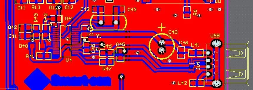
- Press Shift+S to view all routing on a single layer. Right-click the mouse to drag and display the overall layout, and scroll the mouse wheel forward/backward to zoom in or out, which is extremely useful for multilayer board routing.
- When there are a large number of repeated components, use the Align arrangement function. Select the components to be arranged, use the shortcut key shift+ctrl+H for uniform horizontal arrangement, shift+ctrl+V for uniform vertical arrangement, along with shift+ctrl+T and shift+ctrl+B for alignment operations.
- Group operation: Select all components to be operated, hold down Shift and double-click the left mouse button on one of the components to perform unified attribute setting for all selected components.
- Net labels in all schematics within a project are interconnected. If you need to create a top-level sheet and sub-sheets, select Design->Create Sheet Symbol From Sheet or HDL.
- To add a signal layer, go to Design->Layer Stack Manager, select the Top Layer, and then click Add Layer (positive film) or Add Internal Plane (negative film).
- Fanout function: For multi-pin devices such as FPGAs, go to Auto Route ->Fanout->Component, then select the device to be fanned out, and check the options according to actual requirements.
- To back-annotate the modified PCB pin sequence to the schematic, go to Project->Project Option->options, uncheck the Changing Schematic Pins option, and then select Design->Update Schematics in xx.PrjPCB.
- Interactive Routing: That is, modifying the pin sequence of the device, with the following precautions:
a. First, configure the pins that allow swapping: go to Tools->Pin/Part Swapping->Configure, select the chip to be swapped (such as FPGA), then select the IO pins that allow swapping. Clock pins and configuration pins such as nCSO, nCE, ASDO, DATA0 must not be selected for swapping. Check Show Assign IO pin Only, select the target pins, and add them to a group such as the Type group.
b. Check the Pin Swap option to enable pin swapping permission.
c. Go to Tools->Pin/Part Swapping->Interactive Pin/Net Swapping (shortcut key TWI).
- Precautions for multilayer board routing:
a. The track width inside the FPGA shall be ≥4mil (subject to the minimum pitch between pins of the FPGA). The outer diameter of the signal via shall be ≥18mil, with the inner diameter ≥8mil; the outer diameter of the power through-hole shall be 50mil, with the inner diameter 20mil.
b. Length-matched traces: Length matching is required for signals with strict clock synchronization requirements. To view the PCB, go to view->Workspace Panels->PCB->PCB, group the networks to be length-matched for easy track length observation (double-click All Net to add a network group). Go to Tools->Interactive Length Tuning (shortcut key TR), select a track in the network, press Tab to add the target network, and perform length-matched routing with the longest track in the network as the reference. Pre-route the connections and reserve sufficient space before performing length tuning.
c. Differential pairs: Differential pair routing is required for interfaces such as DVI. Go to view->Workspace Panels->PCB->PCB, select Differential Pairs Editor, create the differential pairs to be routed. Alternatively, you can define differential pairs in the schematic first, then go to Tools->Interactive Diff Pair Length Tuning (shortcut key TI), select one track of the pair, press Tab, and perform routing with the longest track of the target differential pair as the reference.
d. Press S+N to select the entire network, which facilitates deletion operations.
e. To fix a component, double-click the component and check the locked option.
- The final inspection of the board is extremely critical, especially the unrouted network inspection. The power supply and ground network inspection before board soldering is also mandatory.
Two final supplementary points:
31. Press L in the PCB editor to directly edit the display and hide status of each layer.
32. Adopt cross-staggered routing as much as possible to reduce signal interference.
About Maxipcb
Maxipcb empowers innovators to turn cutting-edge technologies into reality.
We offer one-stop solutions for design, simulation, testing, PCB manufacturing, component procurement and SMT assembly, enabling efficient development, rapid deployment and risk control across the full product lifecycle.Serving the world in communications, industrial automation, aerospace, automotive, semiconductor and beyond, we build a safer, more connected future together.

