The wiring strategies of high-level PCB are rich and varied, depending on the functions of PCB. This kind of circuit board may involve many different types of signals, from low-speed digital interfaces to multiple high-speed digital interfaces with different signal integrity requirements. This is undoubtedly a challenging task from the perspective of wiring planning and assigning signal layers to each interface.
Blogger: Zachariah Peterson
The wiring strategies of high-level PCB are rich and varied, depending on the functions of PCB. This kind of circuit board may involve many different types of signals, from low-speed digital interfaces to multiple high-speed digital interfaces with different signal integrity requirements. This is undoubtedly a challenging task from the perspective of wiring planning and assigning signal layers to each interface.
When it comes to the wiring strategy of high-level PCB, we have to talk about the pin layout design of many BGA packages. High-pin BGA usually contains many different digital interfaces, especially when the components are typical microprocessors or FPGA. This is one of the most common factors that lead to the increase of PCB layers.
Because high-level PCB design often faces multiple challenges at the same time, this paper will analyze these challenges one by one and share practical strategies that can successfully realize PCB wiring of high-level PCB.
What causes the number of PCB layers to increase?As mentioned in the introduction, the most common factor that leads to the increase of PCB layers is the existence of large BGA components. This kind of component has high density pins at the bottom of the device, and more circuit layers are needed to make the signal reach each pin. Because these components are mostly ASIC, microprocessor or FPGA, they also integrate a large number of digital interfaces with different requirements for signal integrity and wiring, as well as many power and grounding pins.
Many designers are familiar with the simple formula for estimating the number of layers required for full connection of BGA pins. When the solder ball spacing of BGA is large enough (allowing wiring between pins), each signal layer can accommodate two rows of BGA pins:
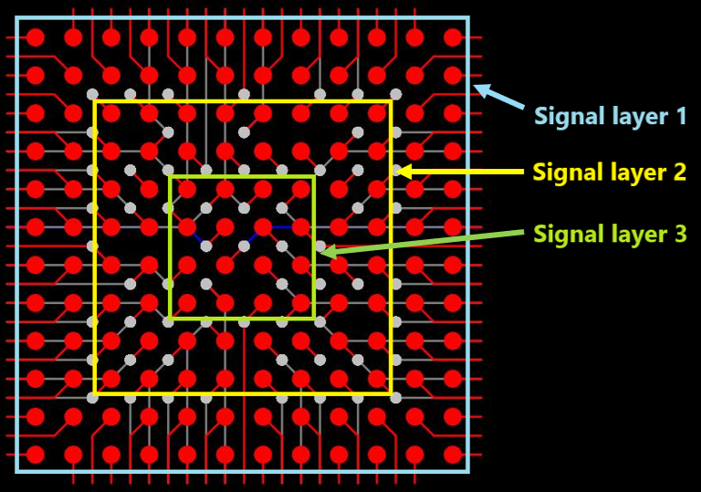
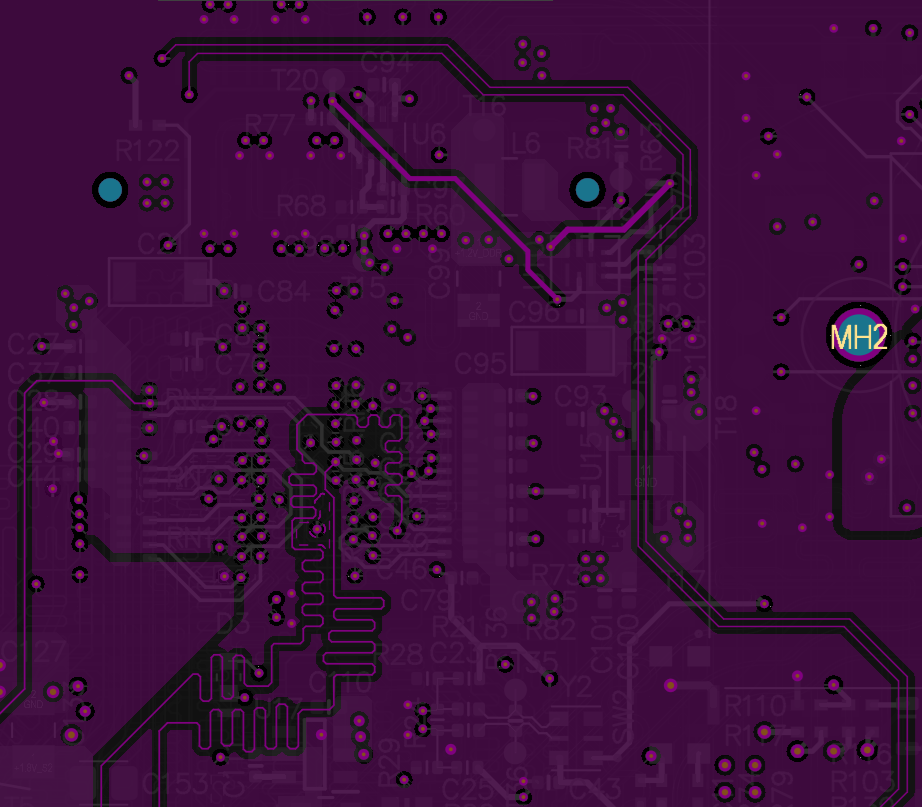
For coarse pitch BGA package (traces can be arranged between solder balls), each layer can be wired with 2 rows/columns of signals. The pad layout of some BGA packages is complex, and there may be missing solder balls in the inner row (as shown in the following figure). The calculation of the number of layers of this kind of BGA is usually different from the above standard BGA.
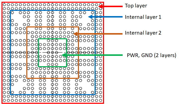
When the pin spacing of components is extremely fine (BGA pads cannot be wired), the required number of layers needs to be doubled; If a large number of pins are power and ground pins, the number of layers will be reduced. In addition, a large number of Quad flat packages (Quad packages) may also lead to high-level demand, but the pin count is usually much lower than that of medium-sized BGA (high-end quad packages have about several hundred pins, while medium-sized BGA has a higher pin count).
Four core routing strategiesStrategy 1: "No strategy"The strategy of "no strategy" is the simplest method so far, and its core is to minimize the number of layers while ensuring routability. Specific implementation methods include: selecting the required number of layers and wiring from BGA by standard fan-out method, compactly arranging all wires with fixed number of layers, or freely wiring and adding new signal layers as required. This strategy applies to the following scenarios:
There is no need to separate different signals into different layers according to impedance specifications.
All interfaces have no impedance requirements (such as serial peripheral interface SPI)
Impedance requirements of all interfaces are consistent.
The number of interfaces with impedance specifications is very small (for example, 1-2).
Although the wiring using this strategy may seem irregular, the number of layers can be effectively controlled by weakening the signal integrity requirements in exchange for routability, and the number of layers can be prevented from being higher than other strategies.
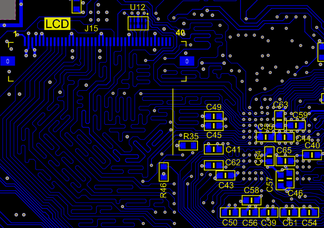
Example: The parallel interface is wired from BGA (lower right corner) and connected to the external LCD module (upper left corner).
Strategy 2: Assign Layers by Interface PriorityIn this strategy, specific impedance-controlled interfaces are assigned special signal layers, and wiring is mainly carried out in these layers. The manufacturer then uses the impedance control method to determine the electrical characteristics used in building the circuit board laminated structure. This strategy can be adopted when there are multiple high-speed interfaces that need impedance control and may have different target impedance values. For some differential interfaces, although their nominal impedance targets are the same, the bandwidth requirements may be different, which requires setting different line widths and spacings for different interfaces. In the following example diagram, the hierarchical distribution of multiple digital interfaces in a 16-layered structure is shown, and the interfaces involved include:
DDR4
CSI-2
1 Gbps LVDS
10 Gbps Ethernet
See how these interfaces are assigned to different layers in the chart below.

Example of high-speed wiring of multi-digital interfaces in high-level PCB You will notice that there are some blank areas on these layers. It should be clear that the main goal of this layered strategy is to make it easier for manufacturers to define impedance specifications. When each layer only corresponds to one impedance specification, manufacturers can more conveniently produce laminated structures that meet each interface impedance target. The disadvantage of this strategy is that it may lead to an increase in the number of layers, and some layers will have unused blank areas. If necessary, you can fill some blank areas with extra ground wire or copper power supply. In some designs, I tend to use these areas to lay copper for power supply, which may even save me a dedicated power supply layer. In addition, you can still use these impedance control layers to transmit low-speed or configuration signals, as long as they are not too close to high-speed traces.
Strategy 3: Separation of high-speed layer and low-speed layerThis strategy is suitable for scenarios where the number of interfaces requiring impedance control is small, or all the impedance controlled interfaces have the same impedance requirements. By separating the signal into dedicated high-speed layer and low-speed layer, a clearer layered design can be realized. This is similar to setting four signal layers in a six-layer board and placing the low-speed signal layers adjacent to each other. This strategy is suitable for orthogonal wiring (the signal direction of adjacent layers is vertical), especially when low-speed signals are distributed in adjacent layers. For example, the wiring in the following example takes an orthogonal direction between components on two different layers:
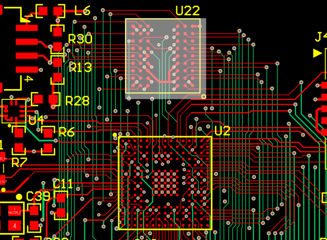
These input/output (I/O) belong to synchronous SDRAM interface, which can be easily connected to the memory chip by orthogonal wiring method. Because of the high proportion of low-speed signals, this strategy faces fewer signal integrity challenges, which helps to maintain a reasonable number of layers and avoid the design complexity caused by excessive layering.
Strategy 4: Common-layer design of power supply and signalIn the design of high-level digital circuit boards, another wiring strategy I often adopt is to integrate some signals and power supply copper on the same layer. The common reason for the increase in the number of layers is not only the huge number of signals or interfaces that need to be wired, but also the increase in the number of layers caused by multiple power channels and power supplies. Novice designers may think that each power channel needs a dedicated power layer, but this will lead to the creation of too many layers and the use of unnecessary copper foil. A better strategy is to draw the power path on the layer in the form of polygon copper laying. In the layer with copper power supply, it is allowed to arrange signal traces, especially low-speed signals or configuration signals. Sample wiring as shown in the following figure:
As long as enough spacing is maintained, it is feasible to wire in the power layer. This method can be used in combination with strategy 2, and the remaining layers that are not allocated to the ground plane are used to arrange low-speed signals, while high-speed signals can still have exclusive layers under strategy 2 as needed. By omitting the dedicated power supply layer and low-speed signal layer, the number of layers is effectively avoided. In addition, traces with controlled impedance can still be arranged in the layer with copper power supply, but spacing rules should be implemented to prevent excessive capacitance from affecting trace impedance. This is consistent with the principle of wiring in coplanar ground plane: avoid using global electrical spacing rules, but create network and layer-specific spacing rules.
About Maxipcb
Maxipcb empowers innovators to turn cutting-edge technologies into reality.
We offer one-stop solutions for design, simulation, testing, PCB manufacturing, component procurement and SMT assembly, enabling efficient development, rapid deployment and risk control across the full product lifecycle.
Serving the world in communications, industrial automation, aerospace, automotive, semiconductor and beyond, we build a safer, more connected future together.


